
Produced 1975 Instruction set 8-bit | Max. CPU clock rate ? MHz to 1.79 MHz Package(s) 40-pin DIP | |
 | ||
Common manufacturer(s) Fairchild Semiconductor | ||
The Fairchild F8 was an 8-bit microprocessor system created by Fairchild Semiconductor announced in 1974, shipped in 1975.
Contents
Features
The engineers who designed the Fairchild F8 Microcomputer did so mindful of a set of goals. The computer needed to be electrically frugal. It needed characteristics that permitted easy interface to standard SSI and MSI components. It needed a moderate instruction set. It needed to be easy to incorporate into a design. The design needed to put the maximum number of computer components and circuits into the LSI components to minimize the package count. This approach reduced the time spent on designing support logic circuits.
These goals resulted in a microcomputer with a multiplexed bus architecture, with just two buses for all functions: the time-multiplexed data bus and a 7-bit control bus for synchronizing the system's components relative to the data bus. The functions of the F8 were distributed among several devices resulting in system simplification.
In the F8 the control bus regulates the use of the data bus through the use of timing signals and state controls. The phi clock divides the machine cycle into discrete phases depending on the instruction being executed. The five state control lines are a function of the instruction being executed. The control bus states regulate the control of information in the computer.
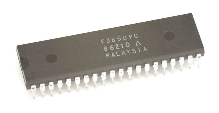
The F3851 is the program storage unit containing 1K ROM. It is programmed in manufacturing using a mask that could be specified by the customer of Fairchild. The F3851A PSU, in the F8 Evaluation Kit 1, was filled with the Fairbug program that allowed inspection and modification of memory, jumping to routines, viewing registers, punching paper tape, and interacting with a teletype user. All 64K of memory could be addressed, and any section could be RAM or ROM. The Fairbug PSU was a demonstration of packing many routines into a 1K ROM.
The program counter (PC) is maintained in the F3851 PSU. There is one program counter for each PSU in the system. Each PSU has a backup program counter. The PSU also contains a pointer register called a data counter, DC. The user only sees one program counter and one data counter.
There are no restrictions in the F8 for how memory addresses are used. They can be either for program or data. Memory interaction has the feature of a Turing machine allowing the computer to put operands in memory and then use the operands as operators.
The F8 has two bidirectional 8-bit ports built into every PSU. An interrupt in the F3850 is similar to a subroutine call. A power-on detection organizes the computer circuitry.
The machine instructions can be grouped into six categories: accumulator instructions, branch instructions, memory reference instructions, address register instructions, scratchpad register instruction, miscellaneous instructions (interrupt, input, output, indirect scratchpad register, load, and store).
Fairbug
The original Fairchild F8 was a set of three interconnected 40-pin ICs. One of the ICs contained a ROM of size 1024 bytes. The ROM entry point during execution of the computer was at the memory address, hexadecimal 8000. At power-on the ROM was entered. The machine instructions in the ROM came to be known as Fairbug (Fairchild Debugger). The Fairbug program is actually a constellation of routines for assisting product development engineers who interacted with Fairbug from a Teletype. The main commands are single ASCII characters drawn from the set {A, B, C, D, E, F, G, I, L, M, N, P, R, S, W}. Register and memory locations were keyed in as parameters immediately after the command identifier. For example, the command M02F0-02FF results in the content of 16 bytes of memory being typed out by the teletype. Fairbug commands address all memory locations and all registers. These locations can be examined or modified by the programmer. Input/output operations are conducted through RAM memory locations. The F8 Development Kit 1 has 1024 bytes of static RAM cells located in the address locations hexadecimal 0000-03FF. Fairbug contains five subroutines which are used in processing commands: Input 2 ASCII Bytes; Output 1 ASCII byte; Output the string CR, LF, Null; Output 1 ASCII byte; Input 1 ASCII Byte from a Parallel Input Device. Fairbug is essentially a random access management routine for all memory, both RAM and ROM, and all registers including program counter, data counter, and scratchpad. The programmer is given the ability to plant any of the 70+ machine code instructions or operands into memory locations. The programmer can then use the G command to load a specific address into the program counter and execute the routine at that address. The objective in providing the Fairbug routines in 1975 was to assist engineers in speeding up the creation of applications for the F8 ICs.
Design
The processor itself had no address bus — memory addresses were kept in each co-processor's own address counter and were manipulated through five control signals, reducing the number of pins and the associated cost. It also featured 64 bytes of scratchpad memory, accessed by the ISAR register in cells (register windows) of eight, which meant external RAM was not always needed for small applications. In addition, the 2-chip processor did not need support chips, unlike others which needed seven or more.
The use of the ISAR register allowed a subroutine to be entered without saving registers, the ISAR would just be changed, speeding execution. Special purpose registers were usually stored in the second cell (regs 8-15), and only the first sixteen registers could be accessed directly. The windowing concept was useful, but only the register pointed to by the ISAR could be accessed — to access other registers, the ISAR was incremented or decremented through the window.
The F8 ran at 1–2 MHz, yielding a 0.5 μs cycle time.
History
The Fairchild F8 microcomputer evolved during 1974 and 1975. The first set of integrated circuits were available to engineers in 1975. These 40-pin integrated circuits required documentation for putting the F8 microcomputer to work. The Preliminary F8 Microcomputer Data Book from Fairchild Semiconductor carries the date June 27, 1975. A Guide to Programming the Fairchild F8 Microcomputer also carries the date June 27, 1975. Another document titled A Timeshare Users Guide for the Fairchild F8 Microcomputer was published August 7, 1975 as Revision A. In September 1975 Fairchild published User's Manual F8 Design Evaluation Kit Number 1. These documents were meant to accompany the Fairchild F8 Design Evaluation Kit 1 which was being sold to engineers. Kit 1 was an 8-bit microprocessor on a single circuit board. The board had three 40-pin ICs: F3850, F3851, F3853. The F3850 held the Central Processing Unit. The F3851 held a Read-Only Memory that contained a program called Fairbug. The F3853 contained circuitry to interface to static random access memory of 64K bytes. The circuit board allowed a simple interface to a Teletype for interacting with the Fairbug program.
The F8 was released in a single-chip implementation (the Mostek 3870) in 1977. According to the CPU Museum, "in 1977 the F8 was the world's leading microprocessor in terms of CPU sales."
The F8 was used in the Fairchild Channel F Video Entertainment System in 1976 and in the VideoBrain Computer system in 1977.
Inventor
The patent document US4086626 lists David H. Chung as the inventor of the computer that we know as the Fairchild F8. The filing date for this patent was June 7, 1976. The invention was an extension of engineering work referred to in the patent under the Priority Date October 7, 1974. The owner of the patent was Fairchild Camera and Instrument Corporation. David H. Chung's career included positions at Texas Instruments, Fairchild, and Sony.