
 | ||
Electron-beam-induced current (EBIC) is a semiconductor analysis technique performed in a scanning electron microscope (SEM) or scanning transmission electron microscope (STEM). It is used to identify buried junctions or defects in semiconductors, or to examine minority carrier properties. EBIC is similar to cathodoluminescence in that it depends on the creation of electron–hole pairs in the semiconductor sample by the microscope's electron beam. This technique is used in semiconductor failure analysis and solid-state physics.
Contents
Physics of the technique
If the semiconductor sample contains an internal electric field, as will be present in the depletion region at a p-n junction or Schottky junction, the electron–hole pairs will be separated by drift due to the electric field. If the p- and n-sides (or semiconductor and Schottky contact, in the case of a Schottky device) are connected through a picoammeter, a current will flow.
EBIC is best understood by analogy: in a solar cell, photons of light fall on the entire cell, thus delivering energy and creating electron hole pairs, and cause a current to flow. In EBIC, energetic electrons take the role of the photons, causing the EBIC current to flow. However, because the electron beam of an SEM or STEM is very small, it is scanned across the sample and variations in the induced EBIC are used to map the electronic activity of the sample.
By using the signal from the picoammeter as the imaging signal, an EBIC image is formed on the screen of the SEM or STEM. When a semiconductor device is imaged in cross-section, the depletion region will show bright EBIC contrast. The shape of the contrast can be treated mathematically to determine the minority carrier properties of the semiconductor, such as diffusion length and surface recombination velocity. In plan-view, areas with good crystal quality will show bright contrast, and areas containing defects will show dark EBIC contrast.
As such, EBIC is a semiconductor analysis technique useful for evaluating minority carrier properties and defect populations.
EBIC can be used to probe subsurface hetero-junctions of nanowires and the properties of minority carriers [1].
EBIC has also been extended to the study of local defects in insulators. For example, W.S. Lau (Lau Wai Shing) developed "true oxide electron beam induced current" in the 1990s. Thus, besides p-n junction or Schottky junction, EBIC can also be applied to MOS diodes. Local defects in semiconductor and local defects in the insulator could be distinguished. There exists a kind of defect which originates in the silicon substrate and extends into the insulator on top of the silicon substrate. (Please see references below.)
Recently, EBIC has been applied to high-k dielectric used in advanced CMOS technology. (Please see references below.)
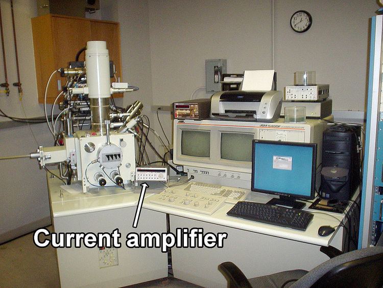
Quantitative EBIC
Most EBIC images are qualitative and only show the EBIC signal as contrast image. Use of an external scan control generator on the SEM and a dedicated data acquisition system allow for sub-picoamp measurements and can give quantitative results. Some systems are commercially available that do this, and provide the ability to provide functional imaging by biasing and applying gate voltages to semiconductor devices.