Kalpana Kalpana (Editor)

ARM Cortex A15

Updated on
Edit
Like
Comment
Share on FacebookTweet on TwitterShare on LinkedInShare on Reddit
Designed by
  
ARM Holdings

Microarchitecture
  
ARMv7-A

Max. CPU clock rate
  
1.0 GHz  to 2.5 GHz

ARM Cortex-A15

Produced
  
In production late 2011, to market late 2012

Min. feature size
  
32 nm/28 nm initially to 22 nm roadmap

Cores
  
1–4 per cluster, 1–2 clusters per physical chip

The ARM Cortex-A15 MPCore is a 32-bit processor core licensed by ARM Holdings implementing the ARMv7-A architecture. It is a multicore processor with out-of-order superscalar pipeline running at up to 2.5 GHz.

Contents

Overview

ARM has claimed that the Cortex-A15 core is 40 percent more powerful than the Cortex-A9 core with the same number of cores at the same speed. The first A15 designs came out in the autumn of 2011, but products based on the chip did not reach the market until 2012.

Key features of the Cortex-A15 core are:

  • 40-bit Large Physical Address Extensions (LPAE) addressing up to 1 TB of RAM. As per the x86 Physical Address Extension, virtual address space remains 32 bit.
  • 15 stage integer/17–25 stage floating point pipeline, with out-of-order speculative issue 3-way superscalar execution pipeline
  • 4 cores per cluster, up to 2 clusters per chip with CoreLink 400 (CCI-400, an AMBA-4 coherent interconnect) and 4 clusters per chip with CCN-504. ARM provides specifications but the licensees individually design ARM chips, and AMBA-4 scales beyond 2 clusters. The theoretical limit is 16 clusters; 4 bits are used to code the CLUSTERID number in the CP15 register (bits 8 to 11).
  • DSP and NEON SIMD extensions onboard (per core)
  • VFPv4 Floating Point Unit onboard (per core)
  • Hardware virtualization support
  • Thumb-2 instruction set encoding to reduce the size of programs with little impact on performance
  • TrustZone security extensions
  • Jazelle RCT for JIT compilation
  • Program Trace Macrocell and CoreSight Design Kit for unobtrusive tracing of instruction execution
  • 32 KB data + 32 KB instruction L1 cache per core
  • Integrated low-latency level-2 cache controller, up to 4 MB per cluster
  • Chips

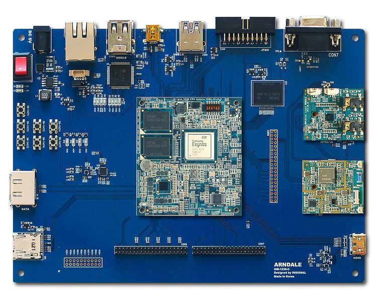
    First implementation came from Samsung in 2012 with the Exynos 5 Dual, which shipped in October 2012 with the Samsung Chromebook Series 3 (ARM version), followed in November by the Google Nexus 10.

    Press announcements of current implementations:

  • Broadcom SoC
  • HiSilicon K3V3
  • Nvidia Tegra 4 (Wayne) and Tegra K1.
  • Samsung Exynos 5 Dual, Quad and Octa
  • ST-Ericsson Nova A9600 (cancelled) (dual-core @ 2.5 GHz over 20k DMIPS)
  • Texas Instruments OMAP 5 SoCs and Sitara AM57x family
  • Other licensees, such as LG, are expected to produce an A15 based design at some point.

    References

    ARM Cortex-A15 Wikipedia


    Similar Topics