
 | ||
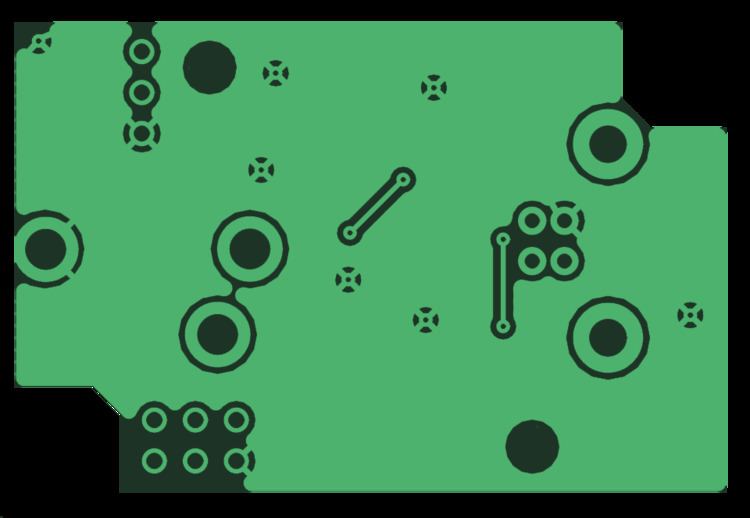
A thermal relief pad is a printed circuit board (PCB) pad connected to a copper pour using a thermal connection. It looks like a normal pad with copper "spokes" connecting it to the surrounding copper.
A typical pad on a printed circuit board is only connected to a few narrow tracks. A pad directly connected to the copper pour is difficult to solder since the heat quickly leaks away from the pad into the copper pour due to high thermal conductivity of copper. A thermal connection restricts the heat flow, making the pad easier to solder. Via holes that only connect one layer to another, without having soldering wires or pins into the hole, do not normally need thermal restriction. Wire leaded components that are either carrying radio frequency currents, where the additional inductance would be problematic, or where very high current densities are expected, and the spokes of the thermal relief may act as a fuse, may require the thermal relief pattern to be customised or even omitted, in which case the parts may require additional hand soldering during assembly.