
 | ||
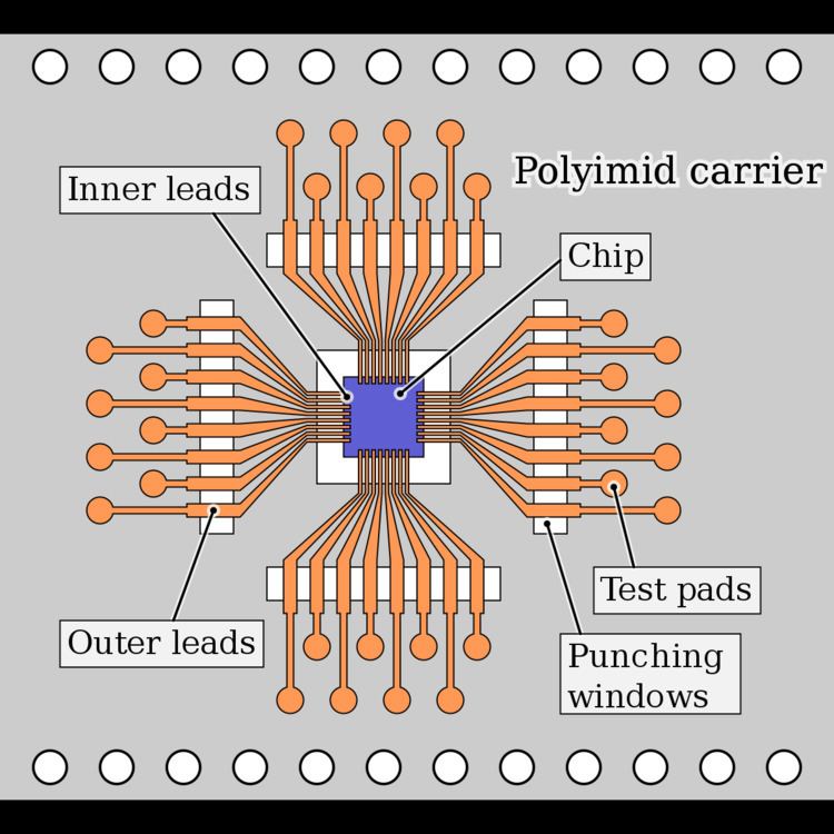
Tape-automated bonding (TAB) is a process that places bare integrated circuits onto a printed circuit board (PCB) by attaching them to fine conductors in a polyamide or polyimide film, thus providing a means to directly connect to external circuits.
Contents
Process
The tape-automated bonding process places bare integrated circuits onto a printed circuit board. The mounting is done such that the bonding sites of the die, usually in the form of bumps or balls made of gold or solder, are connected to fine conductors on the tape, which provide the means of connecting the die to the package or directly to external circuits. Sometimes the tape on which the die is bonded already contains the actual application circuit of the die. The film is moved to the target location, and the leads are cut and soldered as necessary. The bare chip may then be encapsulated ("glob topped") with epoxy or plastic.
Standards
Standard sizes for polyimide tapes include widths of 35 mm, 45 mm, and 70 mm and thicknesses between 50 and 100 micrometers. Since the tape is in the form of a roll, the length of the circuit is measured in terms of sprocket pitches, with each sprocket pitch measuring about 4.75 mm. Thus, a circuit size of 16 pitches is about 76 mm long.
History and background
The process was invented by Frances Hugle. Historically, TAB was created as an alternative to wire bonding and finds common use by manufacturers in LCD display driver circuits.