
 | ||
Surface-mount technology (SMT) is a method for producing electronic circuits in which the components are mounted or placed directly onto the surface of printed circuit boards (PCBs). An electronic device so made is called a surface-mount device (SMD). In the industry it has largely replaced the through-hole technology construction method of fitting components with wire leads into holes in the circuit board. Both technologies can be used on the same board, with the through-hole technology used for components not suitable for surface mounting such as large transformers and heat-sinked power semiconductors.
Contents
- History
- Terms
- Assembly techniques
- Advantages
- Disadvantages
- Rework
- Infrared
- Hot gas
- Rectangular passive components
- Metal electrode leadless face MELF
- Small outline transistor SOT
- Other
- Dual in line
- Quad in line
- Grid arrays
- Non packaged devices
- Resistors
- Capacitors
- Inductors
- Discrete semiconductors
- Integrated circuits
- References
By employing SMT, the production process speeds up, but the risk of defects also increase due to the components miniaturization and denser packing of boards. In those conditions, the failures detection have become critical for any SMT manufacturing process.
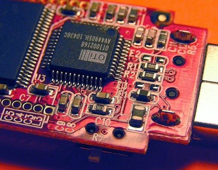
An SMT component is usually smaller than its through-hole counterpart because it has either smaller leads or no leads at all. It may have short pins or leads of various styles, flat contacts, a matrix of solder balls (BGAs), or terminations on the body of the component.
History
Surface mounting was originally called "planar mounting".
Surface-mount technology was developed in the 1960s and became widely used in the late 1980s. Much of the pioneering work in this technology was by IBM. The design approach first demonstrated by IBM in 1960 in a small-scale computer was later applied in the Launch Vehicle Digital Computer used in the Instrument Unit that guided all Saturn IB and Saturn V vehicles. Components were mechanically redesigned to have small metal tabs or end caps that could be directly soldered to the surface of the PCB. Components became much smaller and component placement on both sides of a board became far more common with surface mounting than through-hole mounting, allowing much higher circuit densities. Often only the solder joints hold the parts to the board, in rare cases parts on the bottom or "second" side of the board may be secured with a dot of adhesive to keep components from dropping off inside reflow ovens if the part has a large size or weight. Adhesive is sometimes used to hold SMT components on the bottom side of a board if a wave soldering process is used to solder both SMT and through-hole components simultaneously. Alternatively, SMT and through-hole components can be soldered together without adhesive if the SMT parts are first reflow-soldered, then a selective solder mask is used to prevent the solder holding the parts in place from reflowing and the parts floating away during wave soldering. Surface mounting lends itself well to a high degree of automation, reducing labor cost and greatly increasing production rates. SMDs can be one-quarter to one-tenth the size and weight, and one-half to one-quarter the cost of equivalent through-hole parts.
Terms
Because "surface-mount" refers to a methodology of manufacturing, there are different terms used when referring to the different aspect of the method, which distinguishes for example the components, technique, and machines used in manufacturing. These terms are listed in the following table:
Assembly techniques
Where components are to be placed, the printed circuit board normally has flat, usually tin-lead, silver, or gold plated copper pads without holes, called solder pads. Solder paste, a sticky mixture of flux and tiny solder particles, is first applied to all the solder pads with a stainless steel or nickel stencil using a screen printing process. It can also be applied by a jet-printing mechanism, similar to an inkjet printer. After pasting, the boards then proceed to the pick-and-place machines, where they are placed on a conveyor belt. The components to be placed on the boards are usually delivered to the production line in either paper/plastic tapes wound on reels or plastic tubes. Some large integrated circuits are delivered in static-free trays. Numerical control pick-and-place machines remove the parts from the tapes, tubes or trays and place them on the PCB.
The boards are then conveyed into the reflow soldering oven. They first enter a pre-heat zone, where the temperature of the board and all the components is gradually, uniformly raised. The boards then enter a zone where the temperature is high enough to melt the solder particles in the solder paste, bonding the component leads to the pads on the circuit board. The surface tension of the molten solder helps keep the components in place, and if the solder pad geometries are correctly designed, surface tension automatically aligns the components on their pads. There are a number of techniques for reflowing solder. One is to use infrared lamps; this is called infrared reflow. Another is to use a hot gas convection. Another technology which is becoming popular again is special fluorocarbon liquids with high boiling points which use a method called vapor phase reflow. Due to environmental concerns, this method was falling out of favor until lead-free legislation was introduced which requires tighter controls on soldering. Currently, at the end of 2008, convection soldering is the most popular reflow technology using either standard air or nitrogen gas. Each method has its advantages and disadvantages. With infrared reflow, the board designer must lay the board out so that short components don't fall into the shadows of tall components. Component location is less restricted if the designer knows that vapor phase reflow or convection soldering will be used in production. Following reflow soldering, certain irregular or heat-sensitive components may be installed and soldered by hand, or in large-scale automation, by focused infrared beam (FIB) or localized convection equipment.
If the circuit board is double-sided then this printing, placement, reflow process may be repeated using either solder paste or glue to hold the components in place. If a wave soldering process is used, then the parts must be glued to the board prior to processing to prevent them from floating off when the solder paste holding them in place is melted.
After soldering, the boards may be washed to remove flux residues and any stray solder balls that could short out closely spaced component leads. Rosin flux is removed with fluorocarbon solvents, high flash point hydrocarbon solvents, or low flash solvents e.g. limonene (derived from orange peels) which require extra rinsing or drying cycles. Water-soluble fluxes are removed with deionized water and detergent, followed by an air blast to quickly remove residual water. However, most electronic assemblies are made using a "No-Clean" process where the flux residues are designed to be left on the circuit board [benign]. This saves the cost of cleaning, speeds up the manufacturing process, and reduces waste.
Certain manufacturing standards, such as those written by the IPC - Association Connecting Electronics Industries require cleaning regardless of the solder flux type used to ensure a thoroughly clean board. Even no-clean flux leaves a residue which, under IPC standards, must be removed. Proper cleaning removes all traces of solder flux, as well as dirt and other contaminants that may be invisible to the naked eye. However, while shops conforming to IPC standard are expected to adhere to the Association's rules on board condition, not all manufacturing facilities apply IPC standard, nor are they required to do so. Additionally, in some applications, such as low-end electronics, such stringent manufacturing methods are excessive both in expense and time required.
Finally, the boards are visually inspected for missing or misaligned components and solder bridging. If needed, they are sent to a rework station where a human operator repairs any errors. They are then usually sent to the testing stations (in-circuit testing and/or functional testing) to verify that they operate correctly. Automated Optical Inspection (AOI) systems are commonly used in PCB manufacturing. This technology has proven highly efficient for process improvements and quality achievements.
Advantages
The main advantages of SMT over the older through-hole technique are:
Disadvantages
Rework
Defective surface-mount components can be repaired by using soldering irons (for some connections), or using a non-contact rework system. In most cases a rework system is the better choice because SMD work with a soldering iron requires considerable skill and is not always feasible.
Reworking usually corrects some type of error, either human- or machine-generated, and includes the following steps:
Sometimes hundreds or thousands of the same part need to be repaired. Such errors, if due to assembly, are often caught during the process. However, a whole new level of rework arises when component failure is discovered too late, and perhaps unnoticed until the end user of the device being manufactured experiences it. Rework can also be used if products of sufficient value to justify it require revision or re-engineering, perhaps to change a single firmware-based component. Reworking in large volume requires an operation designed for that purpose.
There are essentially two non-contact soldering/desoldering methods: infrared soldering and soldering with hot gas.
Infrared
With infrared soldering, the energy for heating up the solder joint is transmitted by long- or short-wave infrared electromagnetic radiation.
Advantages:
Disadvantages:
Hot gas
During hot gas soldering, the energy for heating up the solder joint is transmitted by a hot gas. This can be air or inert gas (nitrogen).
Advantages:
Disadvantages:
Surface-mount components are usually smaller than their counterparts with leads, and are designed to be handled by machines rather than by humans. The electronics industry has standardized package shapes and sizes (the leading standardisation body is JEDEC). These include:
The codes given in the chart below usually tell the length and width of the components in tenths of millimeters or hundredths of inches. For example, a metric 2520 component is 2.5 mm by 2.0 mm which corresponds roughly to 0.10 inches by 0.08 inches (hence, imperial size is 1008). Exceptions occur for imperial in the two smallest rectangular passive sizes. The metric codes still represent the dimensions in mm, even though the imperial size codes are no longer aligned. Problematically, some manufacturers are developing metric 0201 components with dimensions of 0.25 mm × 0.125 mm (0.0098 in × 0.0049 in), but the imperial 01005 name is already being used for the 0.4 mm × 0.2 mm (0.0157 in × 0.0079 in) package.
Rectangular passive components
Mostly resistors and capacitors.
Metal electrode leadless face (MELF)
Mostly resistors and diodes; barrel shaped components, dimensions do not match those of rectangular references for identical codes.
Small-outline transistor (SOT)
Other
Small-outline transistor (SOT)
Dual-in-line
Quad-in-line
Grid arrays
Non-packaged devices
Although surface-mount, these devices require specific process for assembly.
There are often subtle variations in package details from manufacturer to manufacturer, and even though standard designations are used, designers need to confirm dimensions when laying out printed circuit boards.
Resistors
For 5% precision SMD resistors usually are marked with their resistance values using three digits: two significant digits and a multiplier digit. These are quite often white lettering on a black background, but other colored backgrounds and lettering can be used.
The black or colored coating is usually only on one face of the device, the sides and other face simply being the uncoated, usually white ceramic substrate. The coated surface, with the resistive element beneath is normally positioned face up when the device is soldered to the board, although they can be seen in rare cases mounted with the uncoated underside face up, whereby the resistance value code is not visible.
For 1% precision SMD resistors, the code is used, as three digits would otherwise not convey enough information. This code consists of two digits and a letter: the digits denote the value's position in the E96 sequence, while the letter indicates the multiplier.
Typical examples of resistance codes
There is an online tool to translate codes to resistance values. Resistors are made in several types; a common types uses a ceramic substrate. Resistance values are available in several tolerances defined in EIA Decade Values Table :
Capacitors
Non electrolytic capacitors are usually unmarked and the only reliable method of determining their value is removal from the circuit and subsequent measurement with a capacitance meter or impedance bridge. The materials used to fabricate the capacitors, such as Nickel Tantalate, possess different colours and these can give an approximate idea of the capacitance of the component.
Generally physical size is proportional to capacitance and voltage^2 for the same dielectric. For example, a 100 nF 50 V capacitor may come in the same package as a 10 nF 150 V device.
SMD (non electrolytic) capacitors, which are usually monolithic ceramic capacitors, exhibit the same body color on all four faces not covered by the end caps.
SMD electrolytic capacitors, usually tantalum capacitors, and film capacitors are marked like resistors, with two significant figures and a multiplier in units of pico Farads or pF, (10−12 Farad.)
Examples
The electrolytic capacitors are usually encapsulated in black or beige epoxy resin with flat metal connecting strips bent underneath. Some film or tantalum electrolytic types are unmarked and possess red, orange or blue body colors with complete end caps, not metal strips.
Inductors
Due to the small dimensions of SMDs, SMT inductors are limited to values of less than about 10 mH. Smaller inductance with moderately high current ratings are usually of the ferrite bead type. They are simply a metal conductor looped through a ferrite bead and almost the same as their through-hole versions but possess SMD end caps rather than leads. They appear dark grey and are magnetic, unlike capacitors with a similar dark grey appearance. These ferrite bead type are limited to small values in the nH (nano Henry), range and are often used as power supply rail decouplers or in high frequency parts of a circuit. Larger inductors and transformers may of course be through-hole mounted on the same board.
SMT inductors with larger inductance values often have turns of wire or flat strap around the body or embedded in clear epoxy, allowing the wire or strap to be seen. Sometimes a ferrite core is present also. These higher inductance types are often limited to small current ratings, although some of the flat strap types can handle a few amps.
As with capacitors, component values and identifiers are not usually marked on the component itself; if not documented or printed on the PCB, measurement, usually removed from the circuit, is the only way of determining them.
Discrete semiconductors
Discrete semiconductors, such as transistors, diodes and FETs are often marked with a two- or three-symbol code in which the same code marked on different packages or on devices made by different manufacturers can translate to different devices.
Many of these codes, used because the devices are too small to be marked with more traditional numbers used on through-hole equivalent devices, correlate to more familiar traditional part numbers when a correlation list is consulted.
GM4PMK in the United Kingdom has prepared a correlation list, and a similar .pdf list is also available, although these lists are not complete.
Integrated circuits
Generally, integrated circuit packages are large enough to be imprinted with the complete part number which includes the manufacturer's specific prefix, or a significant segment of the part number and the manufacturer's name or logo.
Examples of manufacturers' specific prefixes: