Silicon on insulator sapphire
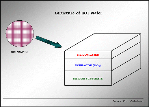
Silicon on insulator (SOI) technology refers to the use of a layered silicon–insulator–silicon substrate in place of conventional silicon substrates in semiconductor manufacturing, especially microelectronics, to reduce parasitic device capacitance, thereby improving performance. SOI-based devices differ from conventional silicon-built devices in that the silicon junction is above an electrical insulator, typically silicon dioxide or sapphire (these types of devices are called silicon on sapphire, or SOS). The choice of insulator depends largely on intended application, with sapphire being used for high-performance radio frequency (RF) and radiation-sensitive applications, and silicon dioxide for diminished short channel effects in microelectronics devices. The insulating layer and topmost silicon layer also vary widely with application.
Contents
- Silicon on insulator sapphire
- 42 oxide isolate cmos control of latch up silicon on insulator soi
- Industry need
- SOI transistors
- Manufacture of SOI wafers
- Use in the microelectronics industry
- Use in high performance radio frequency RF applications
- Use in photonics
- References

42 oxide isolate cmos control of latch up silicon on insulator soi
Industry need

The implementation of SOI technology is one of several manufacturing strategies employed to allow the continued miniaturization of microelectronic devices, colloquially referred to as "extending Moore's Law" (or "More Moore", abbreviated "MM"). Reported benefits of SOI technology relative to conventional silicon (bulk CMOS) processing include:

From a manufacturing perspective, SOI substrates are compatible with most conventional fabrication processes. In general, an SOI-based process may be implemented without special equipment or significant retooling of an existing factory. Among challenges unique to SOI are novel metrology requirements to account for the buried oxide layer and concerns about differential stress in the topmost silicon layer. The threshold voltage of the transistor depends on the history of operation and applied voltage to it, thus making modeling harder. The primary barrier to SOI implementation is the drastic increase in substrate cost, which contributes an estimated 10–15% increase to total manufacturing costs.
SOI transistors

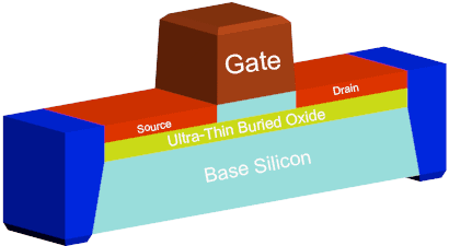
An SOI MOSFET is a semiconductor device (MOSFET) in which a semiconductor layer such as silicon or germanium is formed on an insulator layer which may be a buried oxide (BOX) layer formed in a semiconductor substrate. SOI MOSFET devices are adapted for use by the computer industry. The buried oxide layer can be used in SRAM designs. There are two type of SOI devices: PDSOI (partially depleted SOI) and FDSOI (fully depleted SOI) MOSFETs. For an n-type PDSOI MOSFET the sandwiched p-type film between the gate oxide (GOX) and buried oxide (BOX) is large, so the depletion region can't cover the whole p region. So to some extent PDSOI behaves like bulk MOSFET. Obviously there are some advantages over the bulk MOSFETs. The film is very thin in FDSOI devices so that the depletion region covers the whole film. In FDSOI the front gate (GOX) supports less depletion charges than the bulk so an increase in inversion charges occurs resulting in higher switching speeds. The limitation of the depletion charge by the BOX induces a suppression of the depletion capacitance and therefore a substantial reduction of the subthreshold swing allowing FD SOI MOSFETs to work at lower gate bias resulting in lower power operation. The subthreshold swing can reach the minimum theoretical value for MOSFET at 300K, which is 60mV/decade. This ideal value was first demonstrated using numerical simulation [] []. Other drawbacks in bulk MOSFETs, like threshold voltage roll off, etc. are reduced in FDSOI since the source and drain electric fields can't interfere due to the BOX. The main problem in PDSOI is the "floating body effect (FBE)" since the film is not connected to any of the supplies.
Manufacture of SOI wafers
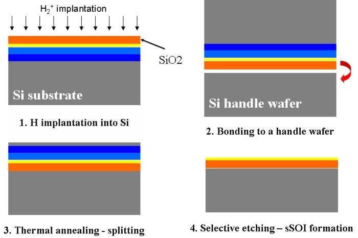
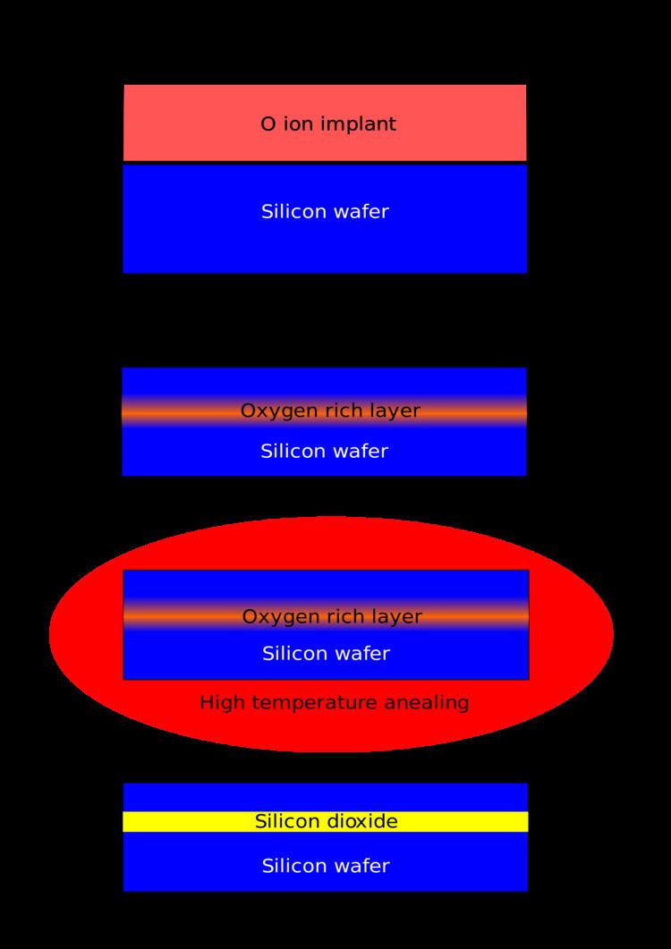
SiO2-based SOI wafers can be produced by several methods:
An exhaustive review of these various manufacturing processes may be found in reference
Use in the microelectronics industry
IBM began to use SOI in the high-end RS64-IV "Istar" PowerPC-AS microprocessor in 2000. Other examples of microprocessors built on SOI technology include AMD's 130 nm, 90 nm, 65 nm, 45 nm and 32 nm single, dual, quad, six and eight core processors since 2001. Freescale adopted SOI in their PowerPC 7455 CPU in late 2001, currently Freescale is shipping SOI products in 180 nm, 130 nm, 90 nm and 45 nm lines. The 90 nm Power Architecture based processors used in the Xbox 360, PlayStation 3 and Wii use SOI technology as well. Competitive offerings from Intel however continues to use conventional bulk CMOS technology for each process node, instead focusing on other venues such as HKMG and Tri-gate transistors to improve transistor performance. In January 2005, Intel researchers reported on an experimental single-chip silicon rib waveguide Raman laser built using SOI.
As for the traditional foundries, on July 2006 TSMC claimed no customer wanted SOI, but Chartered Semiconductor devoted a whole fab to SOI.
Use in high-performance radio frequency (RF) applications
In 1990, Peregrine Semiconductor began development of an SOI process technology utilizing a standard 0.5 μm CMOS node and an enhanced sapphire substrate. Its patented silicon on sapphire (SOS) process is widely used in high-performance RF applications. The intrinsic benefits of the insulating sapphire substrate allow for high isolation, high linearity and electro-static discharge (ESD) tolerance. Multiple other companies have also applied SOI technology to successful RF applications in smartphones and cellular radios.
Use in photonics
SOI wafers are widely used in silicon photonics. The crystalline silicon layer on insulator can be used to fabricate optical waveguides and other passive optical devices for integrated optics. The crystalline silicon layer is sandwiched between the buried insulator (Silicon oxide, Sapphire etc.) and top cladding of air (or Silicon oxide or any other low refractive index material). This enables propagation of electromagnetic waves in the waveguides on the basis of total internal reflection.
