
 | ||
Scanning transmission electron microscopy explained
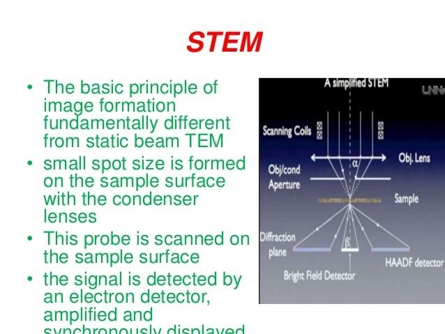
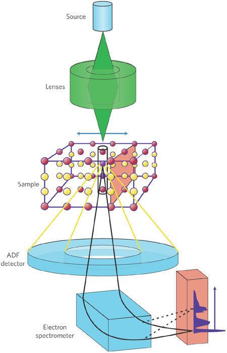
A scanning transmission electron microscope (STEM) is a type of transmission electron microscope (TEM). Pronunciation is [stem] or [esti:i:em]. As with a conventional transmission electron microscope (CTEM), images are formed by electrons passing through a sufficiently thin specimen. However, unlike CTEM, in STEM the electron beam is focused to a fine spot which is then scanned over the sample in a raster. The rastering of the beam across the sample makes STEM suitable for analytical techniques such as Z-contrast annular dark-field imaging, and spectroscopic mapping by energy dispersive X-ray (EDX) spectroscopy, or electron energy loss spectroscopy (EELS). These signals can be obtained simultaneously, allowing direct correlation of images and spectroscopic data.
Contents
- Scanning transmission electron microscopy explained
- History
- Aberration correction
- Applications
- Materials science
- Biology
- Annular dark field
- Bright field
- Universal detectors
- Electron energy loss spectroscopy
- Energy dispersive X ray spectroscopy
- Convergent beam electron diffraction
- Other STEM techniques
- STEM tomography
- Cryo STEM
- In situenvironmental STEM
- Low voltage STEM
- References
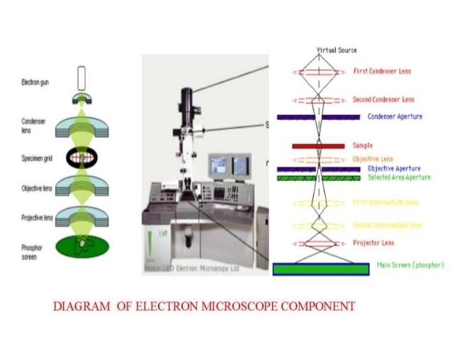
A typical STEM is a conventional transmission electron microscope equipped with additional scanning coils, detectors and necessary circuitry, which allows it to switch between operating as a STEM, or a CTEM; however, dedicated STEMs are also manufactured.
High resolution scanning transmission electron microscopes require exceptionally stable room environments. In order to obtain atomic resolution images in STEM, the level of vibration, temperature fluctuations, electromagnetic waves, and acoustic waves must be limited in the room housing the microscope.
History
In 1925, Louis de Broglie first theorized the wave-like properties of an electron, with a wavelength substantially smaller than visible light. This would allow the use of electrons to image objects much smaller than the previous diffraction limit set by visible light. The first STEM was built in 1938 by Baron Manfred von Ardenne, working in Berlin for Siemens. However, at the time the results were inferior to those of transmission electron microscopy, and von Ardenne only spent two years working on the problem. The microscope was destroyed in an air raid in 1944, and von Ardenne did not return to his work after WWII.
The technique was not developed further until the 1970s, when Albert Crewe at the University of Chicago developed the field emission gun and added a high quality objective lens to create a modern STEM. He demonstrated the ability to image atoms using an annular dark field detector. Crewe and coworkers at the University of Chicago developed the cold field emission electron source and built a STEM able to visualize single heavy atoms on thin carbon substrates.
By the late 1980s and early 1990s, improvements in STEM technology allowed for samples to be imaged with better than 2 Å resolution, meaning that atomic structure could be imaged in some materials.
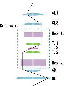
Aberration correction
The addition of an aberration corrector to STEMs enables electron probes to be focused to sub-ångström diameters, allowing images with sub-ångström resolution to be acquired. This has made it possible to identify individual atomic columns with unprecedented clarity. Aberration-corrected STEM was demonstrated with 1.9 Å resolution in 1997 and soon after in 2000 with roughly 1.36 Å resolution. Advanced aberration-corrected STEMs have since been developed with sub-50 pm resolution. Aberration-corrected STEM provides the added resolution and beam current critical to the implementation of atomic resolution chemical and elemental spectroscopic mapping.
Applications
Scanning transmission electron microscopes are used to characterize the nanoscale, and atomic scale structure of specimens, providing important insights into the properties and behaviour of materials and biological cells.
Materials science
Scanning transmission electron microscopy has been applied to characterize the structure of a wide range of material specimens, including semiconductor devices, complex oxides, batteries, fuel cells, catalysts, and 2D materials.
Biology
The first application of STEM to the imaging of biological molecules was demonstrated in 1971. The advantage of STEM imaging of biological samples is the high contrast of annular dark-field images, which can allow imaging of biological samples without the need for staining. STEM has been widely used to solve a number of structural problems in molecular biology.
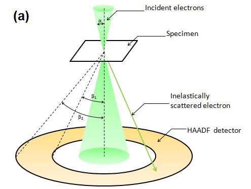
Annular dark-field
In annular dark-field mode, images are formed by fore-scattered electrons incident on an annular detector, which lies outside of the path of the directly transmitted beam. By using a high-angle ADF detector, it is possible to form atomic resolution images where the contrast of an atomic column is directly related to the atomic number (Z-contrast image). Directly interpretable Z-contrast imaging makes STEM imaging with a high-angle detector an appealing technique in contrast to conventional high resolution electron microscopy, in which phase-contrast effects mean that atomic resolution images must be compared to simulations to aid interpretation.
Bright-field
In STEM, bright-field detectors are located in the path of the transmitted electron beam. Axial bright-field detectors are located in the centre of the cone of illumination of the transmitted beam, and are often used to provide complementary images to those obtained by ADF imaging. Annular bright-field detectors, located within the cone of illumination of the transmitted beam, have been used to obtain atomic resolution images in which the atomic columns of light elements such as oxygen are visible.
Universal detectors
Recently, detectors have been developed for STEM that can record a complete convergent beam electron diffraction pattern of all scattered and unscattered electrons at every pixel in a scan of the sample in a large dataset. The data can be analyzed to reconstruct images equivalent to those of any conventional detector geometry, and can be used to map fields in the sample at high spatial resolution, including information about the strain and electric fields.
Electron energy loss spectroscopy
As the electron beam passes through the sample, some electrons in the beam lose energy via inelastic scattering interactions with electrons in the sample. In electron energy loss spectroscopy (EELS), the energy lost by the electrons in the beam is measured using an electron spectrometer, allowing features such as plasmons, and elemental ionization edges to be identified. Energy resolution in EELS is sufficient to allow the fine structure of ionization edges to be observed, which means that EELS can be used for chemical mapping, as well as elemental mapping. In STEM, EELS can be used to spectroscopically map a sample at atomic resolution. Recently developed monochromators can achieve an energy resolution of ~10 meV in EELS, allowing vibrational spectra to be acquired in STEM.
Energy-dispersive X-ray spectroscopy
In energy-dispersive X-ray spectroscopy (EDX) or (EDXS), which is also referred to in literature as X-ray energy dispersive spectroscopy (EDS) or (XEDS), an X-ray spectrometer is used to detect the characteristic X-rays that are emitted by atoms in the sample as they are ionized by electron in the beam. In STEM, EDX is typically used for compositional analysis and elemental mapping of samples. Typical X-ray detectors for electron microscopes cover only a small solid angle, which makes X-ray detection relatively inefficient since X-rays are emitted from the sample in every direction. However, detectors covering large solid angles have been recently developed, and atomic resolution X-ray mapping has even been achieved.
Convergent-beam electron diffraction
Convergent-beam electron diffraction (CBED) is a STEM technique that provides information about crystal structure at a specific point in a sample. In CBED, the width of the area a diffraction pattern is acquired from is equal to the size of the probe used, which can be smaller than 1 Å in an aberration-corrected STEM (see above). CBED differs from conventional electron diffraction in that CBED patterns consist of diffraction disks, rather than spots. The width of CBED disks is determined by the convergence angle of the electron beam. Other features, such as Kikuchi lines are often visible in CBED patterns. CBED can be used to determine the point and space groups of a specimen.
Other STEM techniques
Specialized sample holders, or modifications to the microscope can allow a number of additional techniques to be performed in STEM. Some examples are described below.
STEM tomography
STEM tomography allows the complete three-dimensional internal and external structure of a specimen to be reconstructed from a tilt-series of 2D projection images of the specimen acquired at incremental tilts. High angle ADF STEM is a particularly useful imaging mode for electron tomography because the intensity of high angle ADF-STEM images varies only with the projected mass-thickness of the sample, and the atomic number of atoms in the sample. This yields highly interpretable three dimensional reconstructions.
Cryo-STEM
Cryo-electron microscopy in STEM (Cryo-STEM) allows specimens to be held in the microscope at liquid nitrogen or liquid helium temperatures. This is useful for imaging specimens that would be volatile in high vacuum at room temperature. Cryo-STEM has been used to study vitrified biological samples, vitrified solid-liquid interfaces in material specimens, and specimens containing elemental sulfur, which is prone to sublimation in electron microscopes at room temperature.
In situ/environmental STEM
In order to study the reactions of particles in gaseous environments, a STEM may be modified with a differentially pumped sample chamber to allow gas flow around the sample, whilst a specialized holder is used to control the reaction temperature. Alternatively a holder mounted with an enclosed gas flow cell may be used. Particles and biological cells have been studied in liquid environments in STEM using holders mounted with enclosed liquid cells.
Low-voltage STEM
A low-voltage electron microscope (LVEM) is an electron microscope that is designed to operate at relatively low electron accelerating voltages of between 5 and 25 kV. Some LVEMs can function as an SEM, a TEM and a STEM in a single compact instrument. Using a low beam voltage increases image contrast which is especially important for biological specimens. This increase in contrast significantly reduces, or even eliminates the need to stain biological samples. Resolutions of a few nm are possible in TEM, SEM and STEM modes. The low energy of the electron beam means that permanent magnets can be used as lenses and thus a miniature column that does not require cooling can be used.