
 | ||
For power semiconductor devices (such as BJT, MOSFET, thyristor or IGBT), the safe operating area (SOA) is defined as the voltage and current conditions over which the device can be expected to operate without self-damage.
Contents
- Limits of the safe operating area
- Secondary breakdown
- MOSFET Thermal runaway in linear mode
- Reverse bias safe operating area
- Protection
- References
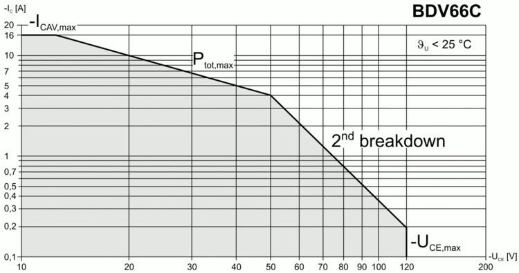
SOA is usually presented in transistor datasheets as a graph with VCE (collector-emitter voltage) on the abscissa and ICE (collector-emitter current) on the ordinate; the safe 'area' referring to the area under the curve. The SOA specification combines the various limitations of the device — maximum voltage, current, power, junction temperature, secondary breakdown — into one curve, allowing simplified design of protection circuitry.
Often, in addition to the continuous rating, separate SOA curves are plotted for short duration pulse conditions (1 ms pulse, 10 ms pulse, etc.).
The safe operating area curve is a graphical representation of the power handling capability of the device under various conditions. The SOA curve takes into account the wire bond current carrying capability, transistor junction temperature, internal power dissipation and secondary breakdown limitations.
Limits of the safe operating area
Where both current and voltage are plotted on logarithmic scales, the borders of the SOA are straight lines:
- IC = ICmax — current limit
- VCE = VCEmax — voltage limit
- IC VCE = Pmax — dissipation limit, thermal breakdown
- IC VCEα = const — this is the limit given by the secondary breakdown (bipolar junction transistors only)
SOA specifications are useful to the design engineer working on power circuits such as amplifiers and power supplies as they allow quick assessment of the limits of device performance, the design of appropriate protection circuitry, or selection of a more capable device. SOA curves are also important in the design of foldback circuits.
Secondary breakdown
For a device that makes use of the secondary breakdown effect see Avalanche transistor
Secondary breakdown is a failure mode in bipolar power transistors. In a power transistor with a large junction area, under certain conditions of current and voltage, the current concentrates in a small spot of the base-emitter junction. This causes local heating, progressing into a short between collector and emitter. This often leads to the destruction of the transistor. Secondary breakdown can occur both with forward and reverse base drive. Except at low collector-emitter voltages, the secondary breakdown limit restricts the collector current more than the steady-state power dissipation of the device. Power MOSFETs do not exhibit secondary breakdown, and their safe operating area is limited only by maximum current (the capacity of the bonding wires), maximum power dissipation and maximum voltage. However, Power MOSFETs have parasitic PN and BJT elements within the structure, which can cause more complex localized failure modes resembling Secondary Breakdown.
MOSFET Thermal runaway in linear mode
In their early history, MOSFETs became known for their absence of secondary breakdown. This benefit was due to the fact that ON-resistance increases with increasing temperature, so that part of the MOSFET which is running hotter (e.g. due to irregularities in the die-attachment etc.) will carry a lower current density, tending to even out any temperature variation and prevent hot spots. Recently, MOSFETs with very high transconductance, optimised for switching operation, have become available. When operated in linear mode, especially at high drain-source voltages and low drain currents, the gate-source voltage tends to be very close to the threshold voltage. Unfortunately the threshold voltage decreases as temperature increases, so that if there are any slight temperature variations across the chip, then the hotter regions will tend to carry more current than the cooler regions when Vgs is very close to Vth. This can lead to thermal runaway and the destruction of the MOSFET even when it is operating within its Vds, Id and Pd ratings. Some (usually expensive) MOSFETs are specified for operation in the linear region and include DC SOA diagrams, e.g. IXYS IXTK8N150L.
Reverse bias safe operating area
Transistors require some time to turn off, due to effects such as minority carrier storage time and capacitance. While turning off, they may be damaged depending on how the load responds (especially with poorly snubbed inductive loads). The reverse bias safe operating area (or RBSOA) is the SOA during the brief time before turning the device into the off state—during the short time when the base current bias is reversed. As long as the collector voltage and collector current stay within the RBSOA during the entire turnoff, the transistor will be undamaged. Typically the RBSOA will be specified for a variety of turn-off conditions, such as shorting the base to the emitter, but also faster turn-off protocols where the base-emitter voltage bias is reversed.
The RBSOA shows distinct dependencies compared to the normal SOA. For example in IGBTs the high-current, high-voltage corner of the RBSOA is cut out when the collector voltage increases too quickly. Since the RBSOA is associated with a very brief turn-off process, it is not constrained by the continuous power dissipation limit.
The ordinary safe operating area (when the device is in the on state) may be referred to as the Forward bias safe operating area (or FBSOA) when it is possible to confuse it with the RBSOA.
Protection
The most common form of SOA protection used with bipolar junction transistors senses the collector-emitter current with a low-value series resistor; the voltage across this resistor is applied to a small auxiliary transistor that progressively 'steals' base current from the power device as it passes excess collector current.
Another style of protection is to measure the temperature of the outside of the transistor, adjust it in software to give the junction temperature, and then if it is too hot turn the device off. Such a protection relies on a micro controller running software. If there is a bank of transistors only a small number need to be sampled for temperature, say ten times a second, to project the bank.
This approach is effective but not bullet-proof. In practice it is very difficult to design a protection circuit that will work under all conditions, and it is left up to the design engineer to weigh the likely fault conditions against the complexity and cost of the protection.