
 | ||
The RCA CDP1802, a 40-pin LSI integrated circuit chip (IC), implemented using COSMAC (Complementary Symmetry Monolithic Array Computer) architecture, is an 8-bit CMOS microprocessor (µP) introduced by RCA in early 1976, the company's first single-chip microprocessor. Within RCA in the early days (ca 1970s), the 1801 and 1802 microprocessors were sometimes referred to as "the COSMAC". Hobbyists usually refer to it simply as "the 1802". It is currently being manufactured by Intersil Corporation as a high-reliability microprocessor. The 1802 has an architecture different from most other 8-bit microprocessors.
Contents
- Introduction
- Radiation Hardening
- Space Technology and Science
- Microcomputer Systems
- Product Integration
- Programming Languages
- Emulators and Simulators
- Chip Suffix Designations
- Registers and IO
- Branching
- Subroutine calls
- Addressing modes
- DMA and Load Mode
- Instruction timing
- Video Graphics
- Code Samples
- References
In 1970 and 1971, Joseph Weisbecker developed a new 8-bit architecture computer system. RCA released Weisbecker's work as the COSMAC 1801U and 1801R (also known as TA6889/TA6890 and TC 1084/TC 1085) in early 1975, using its CMOS process (called COS/MOS, an acronym for Complementary Silicon/Metal-oxide Semiconductor). In 1976, a team led by Jerry Herzog integrated the two chips into one, the 1802.
Successors to the 1802 are the CDP1804, CDP1805, and CDP1806, which have an extended instruction set, other enhanced features (like on-chip RAM and ROM, and built-in Timer), with some versions running at faster clock speeds, though not a significant speed difference. Some features are also lost, like the DMA auto-boot loader functionality. There are also some minor pin function changes.
Introduction
The RCA 1802 has a static core CMOS design with no minimum clock frequency, so that it can be run at very low speeds and low power, including a clock frequency of zero to suspend the microprocessor without affecting its operation. It has two separate 8-pin buses: an 8-bit bidirectional data bus and a time-multiplexed address bus, with the high-order and low-order 8-bits of the 16-bit address being accessed on alternate clock cycles.
The 1802 has a single bit, programmable and testable output port (Q), and four input pins which are directly tested by branch instructions (EF1-EF4).
Its I/O mode is flexible and programmable, and it has a single-phase clock with an on-chip oscillator. Its register set consists of sixteen 16-bit registers. The program counter (PC) can reside in any of these, and is settable using the SEP Rn instruction, providing a simple way to implement multiple PCs, and to perform subroutine calls. (see Subroutine calls below). Similarly, pointers and indirect addressing use the X register (SEX Rn instruction), or the 16 registers can be used as general purpose registers. DMA In and Out and Interrupts use specific registers.
Radiation Hardening
In addition to "bulk silicon" C2L CMOS technology, the 1802 was also available fabricated in Silicon on Sapphire (SOS) semiconductor process technology, which gives it a degree of resistance to radiation and electrostatic discharge (ESD). Along with its extreme low-power abilities, this makes the chip well-suited in space and military applications (also, at the time the 1802 was introduced, very few, if any, other radiation-hardened microprocessors were available in the market). The radiation hardened 1802 version was manufactured at Sandia National Laboratories in agreement with RCA.
Space Technology and Science
The 1802 was used in many spacecraft and space science programs, experiments, projects and modules.
Microcomputer Systems
A number of early microcomputers were based on the 1802, including the COSMAC ELF (1976), Netronics ELF II, Quest SuperELF, COSMAC VIP, Comx-35, Finnish Telmac 1800 and Oscom Nano, Yugoslav Pecom 32 and 64, and the Cybervision systems sold through Montgomery Ward in the late 70s, as well as the RCA Studio II video game console (one of the first consoles to use bitmapped graphics). The Edukit single board computer (SBC) trainer system, similar to an expanded COSMAC Elf, was offered by Modus Systems Ltd. in Britain in the early 1980s. Infinite Incorporated produced an 1802-based, S-100 bus expandable console computer trainer in the late 1970s called the UC1800, available assembled or in kit form.
As part of 1802 Retrocomputing hobbyist work, other computers have been built more recently (post-2000), including the Membership Card microcomputer kit that fits in an Altoids tin and the Spare Time Gizmos Elf 2000 (Elf 2K), among others. See Emulators and Simulators for other systems.
Product Integration
The 1802 was also used in a variety of other products and systems, some science-based, and others commercial.
Programming Languages
The first high-level language available for the 1802 was Forth, provided by Forth, Inc. in 1976. Other available programming languages, both interpreters and compilers, are CHIP-8 (and variants), 8th (a version of Forth created by Lee Hart), Tom Pittman's Tiny BASIC, C, various Assemblers and cross-assemblers, and others. Other specialty languages were used by federal agencies such as NASA and its installations, including Johnson Space Center, AMES, Goddard, Langley, Marshall, and Jet Propulsion Laboratory (JPL), which included the HAL/S cross-compiler, STOIC, a Forth-like language, and others.
Emulators and Simulators
The 1802 chip and computers using the microprocessor have been emulated and simulated in hardware and/or software by hobbyists. One design is in VHDL for an FPGA. A bus-accurate, full speed COSMAC Elf clone was created without a CDP1802 microprocessor chip or CDP1861 video chip using PIC microcontrollers. An online simulator of the COSMAC Elf (enhanced) written in JavaScript runs in the user's browser with no need to download.
Chip Suffix Designations
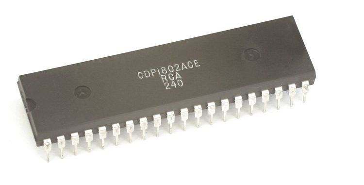
Various suffixes to the CDP1802 part number denote technical specifications, including (A, B, & C) operating speed (3.2 MHz to 6.4 MHz), temperature (-40 °C to +85 °C, -55 °C to +125 °C), and voltage ranges (4V to 10.5V), package type (D, E, Q), and burn-in (X). These were somewhat standardized between the various source suppliers, including RCA, Intersil, Harris, Hughes Aircraft, and Solid State Scientific (SSS). Hughes used the HCMP prefix, and SSS used the SCP (and possibly BCP) prefix, instead of CDP, and had additional suffixes that have not been documented as of yet. (examples: CDP1802A, CDP1802ACE, CDP1802BCD, HCMP1802AP, SCP1802D)
Registers and I/O
The 1802 is an 8-bit byte machine, with minimal support for 16-bit operations, except via 2-byte manipulation. The primary accumulator is the 8-bit 'D' register (Data register). The single bit carry flag is DF (Data Flag). Most operations use the D register, including arithmetic and logic and memory reference load and store instructions. Most 16-bit operations have to work on the lower byte and then the upper byte, via D, using the DF as carry and borrow as needed. Instructions allow the get and put of the upper and lower bytes of the sixteen 16-bit registers via D. However, the 16-bit registers can be incremented and decremented with single instructions, and a few instructions perform automatic increment and decrement, like LDA (load advance) and STXD (store via X and decrement). 16-bit register and value comparisons would also need to use the D register as a go-between, using multiple instructions to perform the operations.
An important feature of the 1802 is the register design of sixteen registers of 16 bits each. Using the SEP instruction, you can select any of the 16 registers to be the program counter; using the SEX instruction, you can select any of the 16-bit registers to be the index register. Register R0 has the special use of holding the memory address for the built-in DMA controller. Register R1 has the special use of being the program counter for the interrupt handler.
The processor has five special I/O lines. There is a single Q output that can be set with the SEQ instruction and reset with the REQ instruction. There are four external, single-bit flag inputs, EF1, EF2, EF3, and EF4, and there are eight dedicated branch instructions to conditionally branch based on the state of those input lines. There are seven Input and seven Output port instructions that utilize the RX register and D accumulator.
The EF and Q lines were typically used for multiple interfaces on 1802-based hobbyist computers because of the lines' favorable and easy handling. It was typical for the Q line to drive a status LED, a cassette interface, an RS-232 interface, and the speaker. This meant that the user could actually hear RS-232 and cassette data being transmitted (unless a volume control was implemented). Traditionally, the EF4 line is attached to the INPUT momentary pushbutton on the COSMAC Elf. Other systems might use one of the other lines.
There are some other special use registers and flags, some internal, and some usable programmatically: 4-bit N, P, X, and I; 8-bit T; and 1-bit IE.
Branching
There are three types of unconditional and conditional branching in the 1802, Short and Long, and Skips.
Short branches are 2-byte instructions, and use 256-byte range, single byte address, page absolute addressing in the range 0 to 255 (hex FF). There is no relative branching. Therefore, care must be taken when attempting to cross page boundaries, which is impossible using short branches, except in two cases. There can be 'side effects', or known usage, when performing a short branch and the short branch instruction or the address byte is the last byte on the page. In this instance, because the PC is incremented after retrieving the byte address, or when the address byte is the first byte of the next page, the PC now points to the next page, not the page in which the branch instruction/byte address is located, so the branch will be in that next page.
Long branches use full 16-bit addressing to support the 64K memory address space, and are the only 3-byte instructions.
Skip instructions increment the PC by one for the unconditional Short Skip, or two for the Long Skips. Only the Long Skip has conditional branching.
Subroutine calls
The processor does not have standard subroutine CALL address and RET instructions, though they can be simulated. The 16-register design makes possible some interesting subroutine call and return mechanisms, though they are better suited to small programs than general purpose coding.
A few commonly used subroutines can be called quickly by keeping their address in one of the 16 registers; however, the called subroutine must know (hard coded) what the calling PC register is to perform the "return" instruction. The SEP instruction is used to call a subroutine pointed to by one of the 16-bit registers and another SEP to return to the caller (SEP stands for Set Program Counter, and selects which one of the 16 registers is to be used as the program counter from that point onward). Before a subroutine returns, it jumps to the location immediately preceding its entry point so that after the SEP "return" instruction returns control to the caller, the register will be pointing to the right value for next usage. (the processor always increments the PC after reference and usage (retrieving the next instruction to execute), so this technique works as noted)
An interesting variation of this scheme is to have two or more subroutines in a ring so that they are called in round robin order. On early hobbyist computers, tricks and techniques like this were commonly used in the horizontal refresh interrupt to reprogram the scan line address to repeat each scan line four times for the video controller.
One well-known and often-used routine is known as SCRT (Standard CALL and RETURN Technique), which allows general purpose subroutine Call and Return, including passing of parameters "in line", and nested subroutines using a stack. Although any of the available registers can be used for this technique, per programmer's preference, many use the routine supplied by RCA in the CDP1802 User Manual, where the suggested register usage is R2 = Stack Pointer, R3 = General Program Counter (PC), R4 = Call, R5 = Return, R6 = Passed Arguments Pointer (non-destructive). Even though these supportive routines are small, there is an execution speed overhead using them. (as opposed to what would be incurred if actual CALL and RET instructions were part of the microprocessor's design) This setup allows R0 to be used for DMA and R1 to be used for Interrupts, if desired, allowing R7 through RF (hex) for general program usage.
Addressing modes
Because of the 16-bit address bus, and the 8-bit data bus, the sixteen general purpose registers are 16 bits wide, but the accumulator D-register is only 8 bits wide. The accumulator, therefore, tends to be a bottleneck. Transferring the contents of one register to another involves four instructions (one Get and one Put on the HI byte of the register, and a similar pair for the LO byte: GHI R1; PHI R2; GLO R1; PLO R2). Similarly, loading a new constant into a register (such as a new address for a subroutine jump, or the address of a data variable) also involves four instructions (two load immediate, LDI, instructions, one for each half of the constant, each one followed by a Put instruction to the register, PHI and PLO).
The two addressing modes Indirect register, and Indirect register with auto-increment are then fairly efficient, to perform 8-bit operations on the data in the accumulator. There are no other addressing modes, though. Thus, the direct addressing mode needs to be emulated using the four instructions mentioned earlier to load the address into a spare register; followed by an instruction to select that register as the index register; followed, finally, by the intended operation on the data variable that is pointed to by that address.
DMA and Load Mode
The CDP1802 has a built-in DMA controller, having two DMA request lines for DMA input and output operations. R0 is used as the DMA address pointer.
The DMA controller also provides a special "load mode", which allows loading of memory while the CLEAR and WAIT inputs of the processor are active. This allows a program to be loaded without the need for a ROM-based bootstrap loader. This was used by the COSMAC Elf microcomputer and its successors to load a program from toggle switches or a hexadecimal keypad with no required software and minimal hardware.
Instruction timing
Clock cycle efficiency is poor in comparison to most 8-bit microprocessors. Eight clock cycles makes up one machine cycle. Most instructions take two machine cycles (16 clock cycles) to execute; the remaining instructions take three machine cycles (24 clock cycles). By comparison, the MOS Technology 6502 takes two to seven clock cycles to execute an instruction, and the Intel 8080 takes four to 18 clock cycles.
Video Graphics
In early 1802-based microcomputers, the companion graphics Video Display Controller chip, CDP1861 (for the NTSC video format, CDP1864 variant for PAL), used the built-in DMA controller to display black and white bitmapped graphics on standard TV screens. The 1861 was also known as the Pixie graphics system, display, chip, and video generator, especially when used with the COSMAC ELF microcomputer. Other known chip markings for the 1861 are TA10171, TA10171V1 and a TA10171X, which were early designations for "pre-qualification engineering samples" and "preliminary part numbers", although they have been found in production RCA Studio II and Netronics Elf microcomputers.
The 1861 chip could display 64 pixels horizontally and 128 pixels vertically, though by reloading the R0 DMA register via the required 1802 software controller program and interrupt service routine, the resolution could be reduced to 64×64 or 64×32 to use less memory or to make square pixels. 64×32 created square pixels and used 256 bytes of memory (2K bits). This was the usual resolution for the Chip-8 game programming system. Since the video graphics frame buffer was often similar or equal in size to the memory size, it was not unusual to display your program/data on the screen allowing you to watch the computer "think" (i.e. process its data). Programs which ran amok and accidentally overwrote themselves could be spectacular.
Although the faster versions of 1802 could operate at 4–5 MHz (at 5 V; it was faster (6.4 MHz) at 10 V), it was usually operated at 3.58 MHz divided by 2 (1.76 MHz) to suit the requirements of the 1861 chip which gave a speed of a little over 100,000 instructions per second.
The CDP1862 Color Generator Circuit IC, an 1861 companion chip, could be used to generate color graphics. Some computer systems, like the Pecom 64, used the VIS (Video Interface System), consisting of the CDP1869 and CDP1870 companion ICs, for somewhat higher resolution color graphics.
Code Samples
This code snippet example is a diagnostic routine that tests ALU (Arithmetic and Logic Unit) Operations.
.. TEST ALU OPS 0000 90 GHI 0 .. SET UP R6 0001 B6 PHI 6 0002 F829 LDI DOIT .. FOR INPUT OF OPCODE 0004 A6 PLO 6 0005 E0 SEX 0 .. (X=0 ALREADY) 0006 6400 OUT 4,00 .. ANNOUNCE US READY 0008 E6 SEX 6 .. NOW X=6 0009 3F09 BN4 * .. WAIT FOR IT 000B 6C INP 4 .. OK, GET IT 000C 64 OUT 4 .. AND ECHO TO DISPLAY 000D 370D B4 * .. WAIT FOR RELEASE 000F F860 LDI #60 .. NOW GET READY FOR 0011 A6 PLO 6 .. FIRST OPERAND 0012 E0 SEX 0 .. SAY SO 0013 6401 OUT 4,01 0015 3F15 BN4 * 0017 E6 SEX 6 .. TAKE IT IN AND ECHO 0018 6C INP 4 .. (TO 0060) 0019 64 OUT 4 .. (ALSO INCREMENT R6) 001A 371A B4 * 001C E0 SEX 0 .. DITTO SECOND OPERAND 001D 6402 OUT 4,02 001F E6 SEX 6 0020 3F20 LOOP: BN4 * .. WAIT FOR IT 0022 6C INP 4 .. GET IT (NOTE: X=6) 0023 64 OUT 4 .. ECHO IT 0024 3724 B4 * .. WAIT FOR RELEASE 0026 26 DEC 6 .. BACK UP R6 TO 0060 0027 26 DEC 6 0028 46 LDA 6 .. GET 1ST OPERAND TO D 0029 C4 DOIT: NOP .. DO OPERATION 002A C4 NOP .. (SPARE) 002B 26 DEC 6 .. BACK TO 0060 002C 56 STR 6 .. OUTPUT RESULT 002D 64 OUT 4 .. (X=6 STILL) 002E 7A REQ .. TURN OFF Q 002F CA0020 LBNZ LOOP .. THEN IF ZERO, 0032 7B SEQ .. TURN IT ON AGAIN 0033 3020 BR LOOP .. REPEAT IN ANY CASENote: The above routine presumes that the CDP1802 microprocessor is in an initial reset state (or that it has been set as such prior to executing this code). Therefore, the program counter (PC) and the X indirect register 'pointer' are both set to 16-bit register R0. That is why you can output an immediate value, as in the example 'OUT 4,00', because PC and X are both pointing to R0. The PC is incremented after the opcode instruction byte is retrieved from memory, so it points to the next address when the OUT 4 is executed. Therefore, it outputs the value in memory pointed to by RX = R0, which is the next immediate byte. The OUT instruction also increments the X register, which is R0, which is also the PC, so it outputs the immediate value after the OUT and continues program execution at the next instruction address after the immediate value. This is why you see the routine set X (SEX) to register R6 and R0 as needed. Also note that, although the OUT opcode increments the RX register, to easily output a section of memory ('buffer'), INP does not. It stores the value at the address pointed to by RX and into the D 8-bit data byte accumulator, but RX is not modified.
The routine also presumes that OUT 4 will display the value in the CPU system's 8-bit LED or 2-digit hex display, and IN 4 gets the value from the eight toggle switches (or possibly the hex keypad). The BN4 opcode (loop; * = 'this address'), "branch if the single-bit input EF4 line is lo", is used to test if the momentary 'Input' pushbutton is pressed. The B4 opcode ('if hi') loop waits for the button to be released. SEQ and REQ turn the single Q line, which is usually attached to an LED, on and off.
The 1802 is a "byte machine", but has 16 16-bit registers, R0-RF (sometimes referred to as 0-F without the 'R' prefix). To deal with 16-bit register data, the programmer must Get and Put the Hi or Lo values of the registers using the D accumulator as the go-between. These high and low bytes of the registers are sometimes referred to as Rn.0 (lo) and Rn.1 (hi). Short Branches are 2-byte opcodes with page-absolute addressing, and a 256-byte address boundary. Long Branches are 3-byte opcodes with full 16-bit address branching.
This information should make the routine more understandable to any computer programmer who is knowledgeable enough to read "pseudo-code" and is minimally familiar with assembly and machine language programming.