
 | ||
A quantum dot display refers to the use of quantum dots (QD), or semiconductor nanocrystals in manufacturing displays. The term carries multiple meanings, including the use of quantum dots to emit light, or merely using them to convert light in LED-backlit LCDs. At present, all commercial products such as TVs advertising quantum dot application branded as QLED are using them only to convert light for LCD backlights, rather than as actual displays.
Contents
- History
- Optical properties of quantum dots
- Quantum dot light emitting diodes
- Fabrication process
- Phase separation
- Contact printing
- Comparison
- References
Authentic quantum dot displays refer to an experimental type of display technology, which is different from those existing commercial products. In these QLEDs, quantum dots (QD) or semiconductor nanocrystals could provide an alternative for commercial applications as electro-optical display technology. This display technology would be similar to organic light-emitting diode (OLED) displays, in that light would be emitted on demand, which would enable more efficient displays, and is also seen as the next generation technology after OLED. However, such products are still experimental. The European Commission does not exempt the use of Cadmium for lighting to create these QLEDs.
Quantum dots in QLEDs could support large, flexible displays and would not degrade as readily as OLEDs, theoretically making them good candidates for flat-panel TV screens, digital cameras, mobile phones and personal gaming equipment.
Properties and performance are determined by the size and/or composition of the QD. QDs are both photo-active (photoluminescent) and electro-active (electroluminescent) allowing them to be readily incorporated into new emissive display architectures.
History
The idea of using quantum dot as a light source emerged in the 1990s. Early applications included imaging using QD infrared photodetectors, light emitting diodes and single-color light emitting devices. Starting from early 2000, scientists started to realize the potential of developing quantum dot for light sources and displays.
A widespread practical application is emerging in so-called Quantum Dot TVs. It must be noted however, that these new TV sets are still LCD TVs as far as picture generation is concerned. QDs are used to improve the LED backlighting - light from a blue LED is converted by QDs to relatively pure red and green, so that this combination of blue, green and red light incurs less absorption of unwanted colors by the color filters behind the LCD screen, thereby increasing useful light throughput and providing a better color gamut. The first TV manufacturer shipping TVs of this kind was Sony in 2013 with Sony's trademark of the technology as Triluminos At the Consumer Electronics Show 2015, Samsung Electronics, LG Electronics, TCL Corporation and Sony showed QD-enhanced LED-backlighting of LCD TVs.
Optical properties of quantum dots
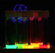
Unlike simple atomic structures, a quantum dot structure has the unusual property that energy levels are strongly dependent on the structure's size. For example, CdSe quantum dot light emission can be tuned from red (5 nm diameter) to the violet region (1.5 nm dot). The physical reason for QD coloration is the quantum confinement effect and is directly related to their energy levels. The bandgap energy that determines the energy (and hence color) of the fluorescent light is inversely proportional to the square of the size of quantum dot. Larger QDs have more energy levels that are more closely spaced, allowing the QD to absorb photons of lower energy (redder color). In other words, the emitted photon energy increases as the dot size decreases, because greater energy is required to confine the semiconductor excitation to a smaller volume.
Quantum dot light-emitting diodes
Quantum-dot-based LEDs (QD-LEDs or QLEDs) are characterized by pure and saturated emission colors with narrow bandwidth. Their emission wavelength is easily tuned by changing the size of the quantum dots. Moreover, QD-LED offer high color purity and durability combined with the efficiency, flexibility, and low processing cost of comparable organic light-emitting devices. QD-LED structure can be tuned over the entire visible wavelength range from 460 nm (blue) to 650 nm (red) (the human eye can detect light from 380 to 750 nm). The emission wavelengths have been continuously extended to UV and NIR range by tailoring the chemical composition of the QDs and device structure.
QLED technology swaps the photoluminescent quantum dots found in current quantum dot TVs for electroluminescent nanoparticles, which means that light can be emitted directly to act as a display, instead of via an LED backlight. Rather than requiring a separate backlight for illumination, an authentic QLED TV natively controls the light emitted by individual pixels.
LCD TVs with quantum dots, branded as "QLED" use BLU (Back-Light Unit) and produce enhanced colors by attaching quantum dot films. On the other hand, genuine QLED TVs would not use BLU and inorganic nano-particles would produce light. However, consumers could be misled by TVs branded as QLED TVs today, as they still use LCDs panels for picture generation. So far, authentic Quantum-dot LED TVs exist in laboratories only.
The structure of a QD-LED is similar to the basic design of an OLED. The major difference is that the light emitting devices are quantum dots, such as cadmium selenide (CdSe) nanocrystals. A layer of quantum dots is sandwiched between layers of electron-transporting and hole-transporting organic materials. An applied electric field causes electrons and holes to move into the quantum dot layer, where they are captured in the quantum dot and recombine, emitting photons. The spectrum of photon emission is narrow, characterized by its full width at half the maximum value.
The challenge of bringing electrons and holes together in small regions for efficient recombination to emit photons without escaping or dissipating was addressed by sandwiching a thin emissive layer between a hole-transporter layer (HTL) and an electron-transport layer (ETL). By making an emissive layer in a single layer of quantum dots, electrons and holes may be transferred directly from the surfaces of the ETL and HTL, providing high recombination efficiency.
So far, most ETLs and HTLs consist of organic materials. Most organic electroluminescent materials favor injection and transport of holes rather than electrons. Thus, the electron-hole recombination generally occurs near the cathode, which could lead to the quenching of the exciton produced. In order to prevent the produced excitons or holes from approaching the cathode, a hole-blocking layer plays dual roles in blocking holes moving towards the cathode and transporting the electrons to the emitting QD layer. Tris-aluminium (Alq3), bathocuproine (BCP), and TAZ are the most commonly used hole-blocking materials. These materials can be used as both electron-transporting layer and hole blocking layer.
For improved electron–hole balance, inorganic transporting layers (e.g., ZnO and TiO2 for ETL, NiO for HTL) have been adopted in QD-LEDs. High efficiency and device performance comparable to that of OLEDs were reported by using the inorganic ZnO ETL. An inverted device structure, stacking the layers inversely (i.e., ETL on the substrate first, and the QD emissive layer, HTL, anode in sequence), was also introduced by using ZnO nanoparticles as ETL.
The array of quantum dots is manufactured by self-assembly in a process known as spin casting: a solution of quantum dots in an organic material is poured onto a substrate, which is then set spinning to spread the solution evenly.
Fabrication process
Quantum dots are solution processable and suitable for wet processing techniques. The two major fabrication techniques for QD-LED are called phase separation and contact-printing.
Phase separation
Phase separation is suitable for forming large-area ordered QD monolayers. A single QD layer is formed by spin casting a mixed solution of QD and TPD. This process simultaneously yields QD monolayers self-assembled into hexagonally close-packed arrays and places this monolayer on top of a co-deposited contact. During solvent drying, the QDs phase separate from the organic under-layer material (TPD) and rise towards the film's surface. The resulting QD structure is affected by many parameters: solution concentration, solvent ration, QD size distribution and QD aspect ratio. Also important is QD solution and organic solvent purity.
Although phase separation is relatively simple, it is not suitable for display device applications. Since spin-casting does not allow lateral patterning of different sized QDs (RGB), phase separation cannot create a multi-color QD-LED. Moreover, it is not ideal to have an organic under-layer material for a QD-LED; an organic under-layer must be homogeneous, a constraint which limits the number of applicable device designs.
Contact printing
The contact printing process for forming QD thin films is a solvent-free method, which is simple and cost efficient with high throughput. During the process, the device structure is not exposed to solvents. Since charge transport layers in QD-LED structures are solvent-sensitive organic thin films, avoiding solvent during the process is a major benefit. This method can produce RGB patterned electroluminescent structures with 1000 ppi (pixels-per-inch) resolution.
The overall process of contact printing:
Contact printing allows fabrication of multi-color QD-LEDs. A QD-LED was fabricated with an emissive layer consisting of 25-µm wide stripes of red, green and blue QD monolayers. Contact printing methods also minimize the amount of QD required, reducing costs. The demonstrated color gamut from QD-LEDs exceeds the performance of both LCD and OLED display technologies.
Comparison
Nanocrystal displays would render as much as a 30% increase in the visible spectrum, while using 30 to 50% less power than LCDs, in large part because nanocrystal displays wouldn't need backlighting. QD LEDs are 50-100 times brighter than CRT and LCD displays, emitting 40,000 cd/m2. QDs are soluble in both aqueous and non-aqueous solvents, which provides for printable and flexible displays of all sizes, including large area TVs. QDs can be inorganic, offering the potential for improved lifetimes compared to OLED (however, since many parts of QD-LED are often made of organic materials, further development is required to improve the functional lifetime.) In addition to OLED displays, pick-and-place microLED displays are emerging as competing technologies to nanocrystal displays.
Other advantages include better saturated green colors, manufacturability on polymers, thinner display and the use of the same material to generate different colors.
However, blue quantum dots require highly precise timing control during the reaction, because blue quantum dots are just slightly above the minimum size. Since sunlight contains roughly equal luminosities of red, green and blue, a display needs to produce approximately equal luminosities of blue, red and green. The human eye requires blue to be about five times more luminous than green, requiring five times more power.