
 | ||
Photonic curing is the high-temperature thermal processing of a thin film using pulsed light from a flashlamp. When this transient processing is done on a low-temperature substrate such as plastic or paper, it is possible to attain a significantly higher temperature than the substrate can ordinarily withstand under an equilibrium heating source such as an oven. Since the rate of most thermal curing processes (drying, sintering, reacting, annealing, etc.) generally increase exponentially with temperature (i.e. they obey the Arrhenius equation), this process allows materials to be cured much more rapidly than with an oven.
Contents
It has become a transformative process used in the manufacture of printed electronics as it allows inexpensive and flexible substrates to be substituted for traditional glass or ceramic substrates. Additionally, the higher temperature processing afforded by photonic curing reduces the processing time exponentially, often from minutes down to milliseconds, which increases throughput all while maintaining a small machine footprint.
Uses
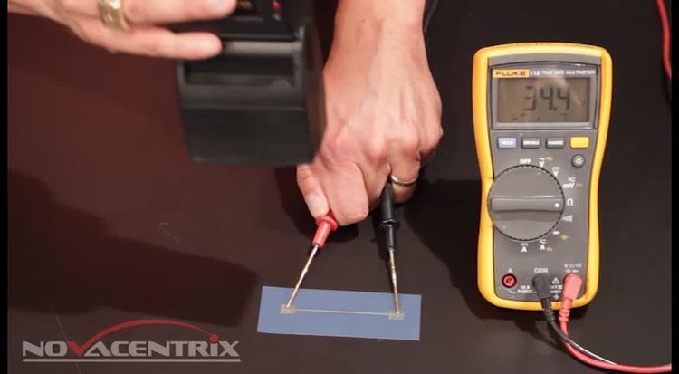
Photonic curing is used as a thermal processing technique in the manufacturing of printed electronics as it allows the substitution of glass or ceramic substrate materials with inexpensive and flexible substrate materials such as polymers or paper. The effect can be demonstrated with an ordinary camera flash. Industrial photonic curing systems are typically water cooled and have controls and features similar to industrial lasers. The pulse rate can be fast enough to allow curing on the fly at speeds beyond 100 m/min making it suitable as a curing process for roll-to-roll processing. Material processing rates can exceed 1 m2/s.
The maturing complexity of modern printed electronics for customer applications demands high throughput manufacturing and improved device function. The functionality of the printed electronics is critically important as customers demand more out of each device. Multiple layers are designed into each device, requiring ever more versatile processing techniques. Photonic curing is uniquely suited to complement the processing needs in the manufacture of modern printed electronics by providing a fast, reliable and transformative processing step. Photonic curing enables a lower thermal processing budget with current materials, and it can provide a path to incorporate more advanced materials and functionality into future printed electronics.
Development
Photonic curing is similar to Pulse Thermal Processing, developed at Oak Ridge National Laboratory, in which a plasma arc lamp is used. In the case of photonic curing, the radiant power is higher and the pulse length is shorter. The total radiant exposure per pulse is less with photonic curing, but the pulse rate is much faster.
Photonic Curing was developed by Nanotechnologies, Inc. (now NovaCentrix) and is incorporated into their PulseForge tools. Xenon Corporation markets photonic curing machines under the brand name Sinteron. Solayer GmbH also markets capabilities based on Flash Lamp Annealing (FLA) for a wide range of industries that include display, PV, semiconductor, printed electronics and architectural glass.. The modular FLA for industry and standalone FLA for R & D improve thin-film layer properties significantly. Photonic curing was introduced at the 2006 NSTI conference and is sometimes referred to as “photonic sintering” since the first application was the sintering of nanosilver and nanocopper inks to form conductive traces on plastic and paper. In addition to sintering metals and ceramics, photonic curing is also used to dry thin films, modulate chemical reactions, and anneal semiconductors such as amorphous silicon. Beside semiconductor applications also large area substrates are being post treated by flash lamp annealing systems, like in the architectural glass coating or display manufacturing industry. Therefore large flash lamp annealing systems with a single tube length up to 3.8 m can be used instead of furnace annealing. The 3.8 m tubes (with arc length of 3.72 m) are the longest flash lamps ever manufactured.