
Produced 2001 Max. CPU clock rate 1.1 GHz to 1.9 GHz Cores 2 | Designed by IBM Min. feature size 180 nm to 130 nm | |
 | ||
Instruction set PowerPC (PowerPC v.2.00/01) | ||
The POWER4 is a microprocessor developed by International Business Machines (IBM) that implemented the 64-bit PowerPC and PowerPC AS instruction set architectures. Released in 2001, the POWER4 succeeded the POWER3 and RS64 microprocessors, and was used in RS/6000 and AS/400 computers, ending a separate development of PowerPC microprocessors for the AS/400. The POWER4 was a multicore microprocessor, with two cores on a single die, the first non-embedded microprocessor to do so. POWER4 Chip was first commercially available multiprocessor chip. The original POWER4 had a clock speed of 1.1 and 1.3 GHz, while an enhanced version, the POWER4+, reached a clock speed of 1.9 GHz. The PowerPC 970 is a derivative of the POWER4.
Contents
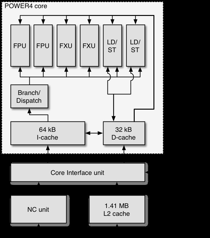
Functional layout
The POWER4 has a unified L2 cache, divided into three equal parts. Each has its own independent L2 controller which can feed 32 bytes of data per cycle. The Core Interface Unit (CIU) connects each L2 controller to either the data cache or instruction cache in either of the two processors. The Non-Cacheable (NC) Unit is responsible for handling instruction serializing functions and performing any noncacheable operations in the storage topology. There is an L3 cache controller, but the actual memory is off-chip. The GX bus controller controls I/O device communications, and there are two 4-byte wide GX buses, one incoming and the other outgoing. The Fabric Controller is the master controller for the network of buses, controlling communications for both L1/L2 controllers, communications between POWER4 chips {4-way, 8-way, 16-way, 32-way} and POWER4 MCM’s. Trace-and-Debug, used for First Failure Data Capture, is provided. There is also a Built In Self Test function (BIST) and Performance Monitoring Unit (PMU). Power-on reset (POR) is supported.
Execution units
The POWER4 implements a superscalar microarchitecture through high-frequency speculative out-of-order execution using eight independent execution units. They are: two floating-point units (FP1-2), two load-store units (LD1-2), two fixed-point units (FX1-2), a branch unit (BR), and a conditional-register unit (CR). These execution units can complete up to eight operations per clock (not including the BR and CR units):
The pipeline stages are:
Multi-chip configuration
The POWER4 also came in a configuration using a multi-chip module (MCM) containing four POWER4 dies in a single package, with up to 128 MB of shared L3 ECC cache per MCM.
POWER4+
The POWER4+ was an improved version of the POWER4 that ran at up to 1.9 GHz. It contained 184 million transistors, measured 267 mm2, and was fabricated in a 0.13 µm SOI CMOS process with eight layers of copper interconnect.