
 | ||
The operational amplifier integrator is an electronic integration circuit. Based on the operational amplifier (op-amp), it performs the mathematical operation of integration with respect to time; that is, its output voltage is proportional to the input voltage integrated over time.
Contents
Applications
The integrator circuit is mostly used in analog computers, analog-to-digital converters and wave-shaping circuits. A common wave-shaping use is as a charge amplifier and they are usually constructed using an operational amplifier though they can use high gain discrete transistor configurations.
Design
The input current is offset by a negative feedback current flowing in the capacitor, which is generated by an increase in output voltage of the amplifier. The output voltage is therefore dependent on the value of input current it has to offset and the inverse of the value of the feedback capacitor. The greater the capacitor value, the less output voltage has to be generated to produce a particular feedback current flow.
The input impedance of the circuit is almost zero because of the Miller effect. Hence all the stray capacitances (the cable capacitance, the amplifier input capacitance, etc.) are virtually grounded and they have no influence on the output signal.
The circuit operates by passing a current that charges or discharges the capacitor Cf during the time under consideration, which strives to retain the virtual ground condition at the input by off-setting the effect of the input current. Referring to the above diagram, if the op-amp is assumed to be ideal, nodes v1 and v2 are held equal, and so v2 is a virtual ground. The input voltage passes a current
The circuit can be analyzed by applying Kirchhoff's current law at the node v2, keeping ideal op-amp behaviour in mind.
Furthermore, the capacitor has a voltage-current relationship governed by the equation:
Substituting the appropriate variables:
Integrating both sides with respect to time:
If the initial value of vo is assumed to be 0 V, this results in a DC error of:
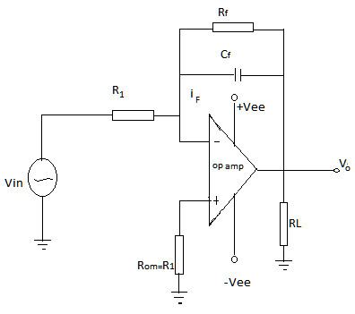
Practical circuit
The ideal circuit is not a practical integrator design for a number of reasons. Practical op-amps have a finite open-loop gain, an input offset voltage and input bias currents (
The input bias current thus causes the same voltage drops at both the positive and negative terminals.
Also, in a DC steady state, the capacitor acts as an open circuit. The DC gain of the ideal circuit is therefore infinite (or in practice, the open-loop gain of a non-ideal op-amp). To counter this, a large resistor
where
The frequency responses of the practical and ideal integrator are shown in the above figure. For both circuits, the crossover frequency
The 3 dB cutoff frequency
The practical integrator circuit is equivalent to an active first-order low-pass filter. The gain is relatively constant up to the cutoff frequency and decreases by 20 dB per decade beyond it. The integration operation occurs for frequencies in the range