
 | ||
Electromagnetic near-field scanner is a measurement system to determine a spatial distribution of an electrical quantity provided by a single or multiple field probes acquired in the near-field region of a device under test possibly accompanied by the associated numerical post-processing methods enabling a conversion of the measured quantity into electromagnetic field.
Contents
Depending on a signal receiver detecting the probe signal, voltage as a function of time or frequency is a typical measured quantity. It should be underlined that as the DUT may be considered any object radiating or storing electromagnetic field energy intentionally or unintentionally, e.g. the antenna radiation excited beyond its resonance frequency. The voltage pattern is usually mapped on planar, cylindrical or spherical geometrical surfaces as a collection of a finite number of spatial samples.
Antenna near-field scanner
First scanners were built in the 1950s to map probe signal variations in front of microwave antennas. Determination of a far-field radiation pattern constitutes the primary application of antenna near-field scanners. This novel technique offered an attractive alternative to conventional open area test sites for measurements of high gain, electrically large antennas or antenna arrays (gain > 20 dBi, diameter > 5λ) in an indoor, controlled and all-weather capability environment. Among well recognized and analyzed errors of the near-field measurements, multiple reflections between an antenna under test (AUT) and an electromagnetically non-transparent field detection system (scatterer) belong to the most contributing errors when the AUT has a high gain. Therefore, the scanning surface is recommended to be located outside the reactive near-field region of the AUT.
EMI near-field scanner
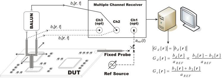
In EMI applications, the main focus of a scanner system is on localization of real electromagnetic interference (EMI) sources distributed in a DUT. Accordingly, the scanning surface is located in the highly reactive region of the DUT to enable a relative spatial localization of the electric charges and current surface densities directly from the mapped pattern of probe signals. Typically the separation between the scanning surface and the DUT is much smaller as the largest geometrical dimension of the DUT. Exemplary distances are 1 mm for scanning of PCBs and 30 μm for scanning of integrated circuits on a die level. In order to quickly localize field emission in frequency domain, time domain detection techniques together with signal processing based on fast Fourier transform could be employed, e.g. utilizing a digital storage oscilloscope as a signal receiver.