
 | ||
Nanoprobing is method of extracting device electrical parameters through the use of nanoscale tungsten 钨wires, used primarily in the semiconductor industry. The characterization of individual devices is instrumental to engineers and integrated circuit designers during initial product development and debug. It is commonly utilized in device failure analysis laboratories to aid with yield enhancement, quality and reliability issues and customer returns. Commercially available nanoprobing systems are integrated into either a vacuum-based scanning electron microscope (SEM) or atomic force microscope (AFM). Nanoprobing systems that are based on AFM technology are referred to as Atomic Force nanoProbers (AFP).
Contents
Principles and operation
AFM based nanoprobers, enable up to eight probe tips to be scanned to generate high resolution AFM topography images, as well as Conductive AFM, Scanning Capacitance, and Electrostatic Force Microscopy images. Conductive AFM provides pico-amp resolution to identify and localize electrical failures such as shorts, opens, resistive contacts and leakage paths, enabling accurate probe positioning for current-voltage measurements. AFM based nanoprobers enable nanometer scale device defect localization and accurate transistor device characterization without the physical damage and electrical bias induced by high energy electron beam exposure.
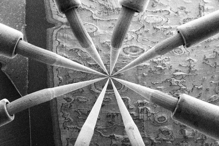
For SEM based nanoprobers, the ultra-high resolution of the microscopes that house the nanoprobing system allow the operator to navigate the probe tips with precise movement, allowing the user to see exactly where the tips will be landed, in real time. Existing nanoprobe needles or “probe tips” have a typical end-point radius ranging from 5 to 35 nm. The fine tips enable access to individual contacts nodes of modern IC transistors. Navigation of the probe tips in SEM based nanoprobers are typically controlled by precision piezoelectric manipulators. Typical systems have anywhere from 2 to 8 probe manipulators with high end tools having better than 5 nm of placement resolution in the X, Y & Z axes and a high accuracy sample stage for navigation of the sample under test.
Application and capabilities for semiconductor devices
Common nanoprobing techniques include, but are not limited to:
Challenges
Common issues that arise: