
 | ||
Low Power flip-flops are becoming important for implementing low power devices. They are essentially Flip-flop (electronics) but with additional features that ensure low power consumption of the flip flop.
Contents
Motivation
In most VLSI devices, maximum power dissipation is due to the clock network and clocked sequential elements. It can account to anywhere between 25% - 40% of the total power according to the variation of parameters like clock frequency, deeper pipelining etc. in a design. Sequential elements, latches and flip flops dissipate power when there is switching in their internal capacitance. This may happen with every clock transition/pulse into the sequential element. Sometimes the sequential elements need to change their state, but sometimes they retain their state and their output remains the same, before and after the clock pulse. This leads to unnecessary dissipation of power due to clock transition. If flip flops are designed in such a way that they are able to gate the clock with respective to their own internal data path, only to use the clock when needed, power dissipation can be brought down.
Conditional Pre-charging Technique
This technique is used for controlling the internal node in the pre charging path in a sequential element. It has been seen to reduce the system power. Referring to Fig1, we can see that the D input is given to the first NMOS in the PDN network (CMOS). When this input is high, the output should be high too. The clk input to the PMOS will charge the output node to high when clk is low. If D input is already high, there is no need to charge the output to high again. Thus, if one can control this behaviour there can be a power reduction in the flop. To control the internal node in the precharge path, a control switch is used as shown in Fig 1. Only a transition that is going to change the state of the output is allowed. As one of the input to flops is the clock, considering the clock (Clock signal) is the element that makes the most transition in a system, a technique such as conditional precharging can significantly help reduce power.
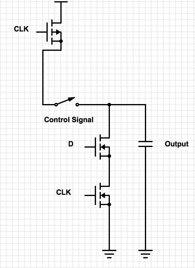
Conditional Capture
This technique looks to prevent any necessary internal node transition by looking at the input and output and checking to see if there is at all a need to switch states. From Fig2, we can see there is a control signal that is applied to control the switching of the internal nodes. We can see the clock is supplied to two NMOS in series. The discharge path will not be complete till the control signal allows the last NMOS to be on. This control signal could be generated by a simple circuitry, with its inputs being the present output, input and the state of the clock (high or low). If the output of the flop is low, and high clock pulse is applied with the input being a low pulse, then there is no need to cause a state transition. The extra computation to sample the inputs cause an increase in setup time of the flop, this is a disadvantage of this technique. A further insight into this technique has been explained well in the journal "High-Performance and Low-Power Conditional Discharge Flip-Flop" by Tarek K. Darwish and Magdy A. Bayoumi.
Data Transition Look-Ahead Flip-Flop
In Fig3, the circuit shows how data transition technique can be beneficial for power saving. The XNOR logical function is performed on the input of the D Flip-Flop and the output Q. When Q and D are equal, output of the logical XNOR will be zero thereby gating the internal clock and generating no internal clock. Referring to Fig3, we can see that the circuit can be broken down into 3 parts, namely data-transition look ahead, pulse generator, clock generator. The pulse generator output is given into the clock generator which is used to clock the D flip Flop. Based on the input and output signals, if there is a need to change the state of the D flop then the clock is allowed to switch to cause a transition else the clock is not allowed to transition. When the clock is not to make a transition, some time has been already spent in computing the logic and data from the D input may make it through the first stage of the D flop and some power is consumed. this power consumption is still less than what an ordinary flop would have consumed with a clock transition and no change in output. As it can be noticed the pulse generator is still generating pulse at every external clock edge. This too can be controlled and a technique that controls this part of the circuit is Clock On Demand.
Clock On Demand Flip Flop
Fig4 shows the COD (Clock On Demand) technique. The clock generator and pulse generator are combined together in this implementation. The advantage of this is that there is reduction in areas and thus more energy efficiency. If the XNOR output is zero then the pulse generator will not generate any internal signal from derived by the external clock. If the output Q and input D do not match then the pulse generator will generate internal clock to aid state transition and change value of output.