
 | ||
Integrated circuits are put into protective packages to allow easy handling and assembly onto printed circuit boards and to protect the devices from damage. A very large number of different types of package exist. Some package types have standardized dimensions and tolerances, and are registered with trade industry associations such as JEDEC and Pro Electron. Other types are proprietary designations that may be made by only one or two manufacturers. Integrated circuit packaging is the last assembly process before testing and shipping devices to customers.
Contents
- Through hole packages
- Chip carrier
- Ball grid array
- Transistor diode small pin count IC packages
- Package dimensions
- Multi chip packages
- References
Occasionally specially-processed integrated circuit dies are prepared for direct connections to a substrate without an intermediate header or carrier. In flip chip systems the IC is connected by solder bumps to a substrate. In beam-lead technology, the metallized pads that would be used for wire bonding connections in a conventional chip are thickened and extended to allow external connections to the circuit. Assemblies using "bare" chips have additional packaging or filling with epoxy to protect the devices from moisture.
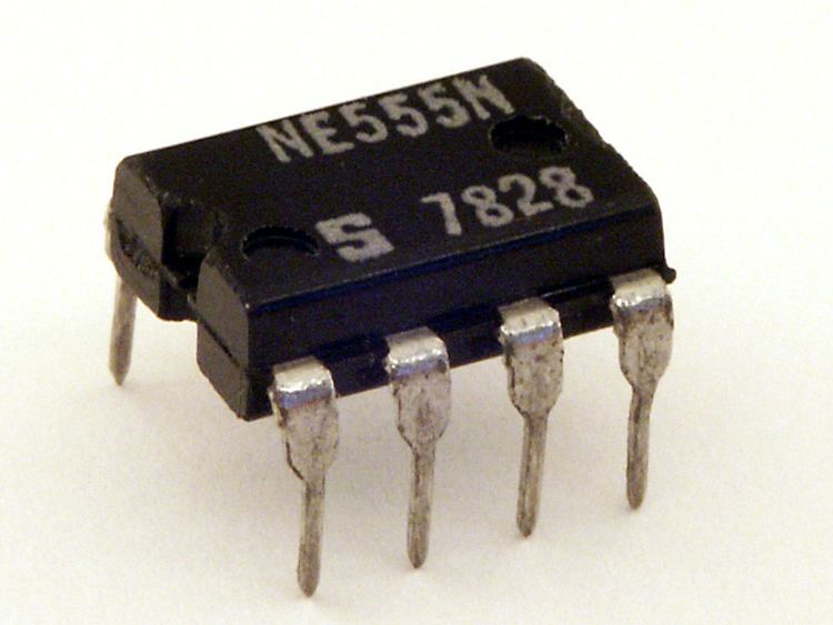
Through-hole packages
Through hole technology uses holes drilled through the PCB for mounting the components. The component has leads that are soldered to pads on the PCB to electrically and mechanically connect them to the PCB.
Chip carrier
A chip carrier is a rectangular package with contacts on all four edges. Leaded chip carriers have metal leads wrapped around the edge of the package, in the shape of a letter J. Leadless chip carriers have metal pads on the edges. Chip carrier packages may be made of ceramic or plastic and are usually secured to a printed circuit board by soldering, though sockets can be used for testing.
Ball grid array
Ball Grid Array BGA uses the underside of the package to place pads with balls of solder in grid pattern as connections to PCB.
Transistor, diode, small pin count IC packages
Package dimensions
All measurements below are given in mm. To convert mm to mils, divide mm by 0.0254 (i.e., 2.54 mm / 0.0254 = 100 mil).
Multi-chip packages
Occasionally people put several chips of silicon in a single package. A variety of techniques for interconnecting several chips within a single package have been proposed and researched: