
 | ||
A Josephson voltage standard is a complex system that uses a superconductive integrated circuit chip operating at 4 K to generate stable voltages that depend only on an applied frequency and fundamental constants. It is an intrinsic standard in the sense that it does not depend on any physical artifact. It is the most accurate method to generate or measure voltage and, by international agreement, is the basis for voltage standards around the World.
Contents
The Josephson effect
In 1962, Brian Josephson, a graduate student at Cambridge University, derived equations for the current and voltage across a junction consisting of a thin insulating barrier separating two superconductors – now generally known as a Josephson junction. His equations predicted that if a junction is driven at frequency
where
The Josephson effect was initially used to improve the measurement of the constant
Early Josephson standards
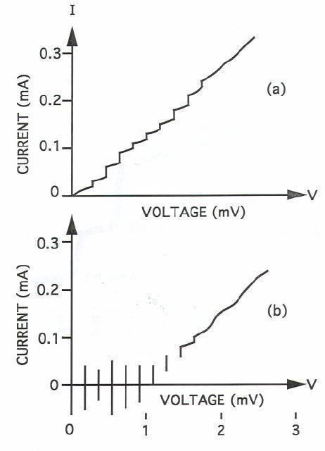
Although the ac Josephson effect provides a much more stable voltage reference than Weston cells, the first single-junction Josephson standards were difficult to use because they generated very small voltages (1-10 mV). Several attempts were made to raise the voltage by connecting two or more junctions in series. The most ambitious of these used 20 junctions in series to realize a voltage of 100 mV with an uncertainty of a few parts in 109. Ensuring that every junction was on a constant voltage step required individually adjusting the bias current to each of the 20 junctions. The difficulty of this procedure makes arrays of significantly more than 20 junctions impractical.
In 1977, Levinson et al. made a suggestion that would ultimately lead to a solution to the multiple-bias problem. Levinson pointed out the importance of the parameter
After several preliminary experiments, a joint effort in 1984 between the National Bureau of Standards in the U. S. and the Physikalisch-Technische Bundes-Anstalt in Germany resolved the problems of junction stability and microwave distribution and created the first large Josephson array based on Levinson's idea. Further design improvements and system development produced the first practical 1 V Josephson standards in 1985. Advances in superconductive integrated circuit technology, largely driven by the quest for a Josephson junction computer, soon made possible much larger arrays. In 1987, the design was extended to a chip with 14484 junctions that generated about 150 000 quantized voltages spanning the range from -10 V to +10 V. Numerous further refinements were made as 10 V Josephson standards were implemented in many national standards laboratories. By 1989, all of the hardware and software for a complete voltage metrology system was commercially available. Today, there are Josephson array voltage standards in more than 70 national, industrial, and military standards laboratories around the world. A program of international comparisons carried out by the Bureau International des Poids et Mesures (BIPM) has measured differences between a traveling Josephson standard and those of NMI’s that are typically less than 1 part in 109.
Junction design details
Figure 3 illustrates the basic structure of one junction in a large series array. The junction is an overlap between two superconductive thin films that are separated by a thin oxide barrier. The junction sits above a ground plane and is separated from it by a few micrometers of insulation. A dc current
-
L must be small enough that the flux induced through the junction area by the microwave magnetic field is much less than the flux quantumh / 2 e - Both
W andL must be small enough that the lowest resonant cavity mode of the junction is greater thanf - To avoid chaotic behavior, the junction plasma frequency
f p J f . - The junction's critical current
I c = W L J should be as large as possible to prevent noise-induced quantum step transitions.
If any of these conditions is violated, the junction voltage is likely to switch randomly among several steps, making measurements impossible. A rigorous derivation of these conditions is the subject of several papers by Kautz.
Figure 4 illustrates the region of stable behavior in the three-dimensional space of
Array Design
The I-V curve shown in Fig. 1b shows steps covering the range from about -1 mV to +1 mV and is for a junction driven by a nearly optimum level of microwave current. At lower microwave current the steps cover a smaller range of voltage and at higher microwave current the steps become smaller and begin to move off the zero current axis. In a large array, every junction must generate a large zero crossing step and thus the microwave power must be adjusted to a value low enough to accommodate the one junction receiving the largest microwave drive. Thus, in order to obtain the largest voltage from the smallest number of junctions, an array standard requires a circuit design that can deliver nearly uniform microwave power to many thousands of junctions, all of which are connected in series. The solution to this problem is a simple extension of Fig. 3 to a series of junctions in a line over a ground plane as shown in Fig. 5a. This results in a microwave stripline that can propagate microwave power with relatively low loss. The capacitive impedance of the junctions is so small (approximately 1 m Ω ) relative to the strip line impedance (approx. 3 Ω) that each junction has a very minor effect on the propagation of microwave power in the strip line. Typically, each junction will absorb about 0.02% to 0.04% of the power propagating through it. It is thus possible to connect several thousand junctions in series and still achieve a power uniformity of about ±1.5 dB. With careful design, striplines with as many as 4800 junctions have been used.
Because 10 V Josephson standards require about 20 000 junctions, it is necessary to adopt a series/parallel circuit similar to that shown in Fig. 5b.[39] Here, a network of low- and high-pass filters allow the microwave power to be split into four parallel paths while maintaining a dc path in which all junctions are connected in series.
A typical integrated circuit layout for an array of 20 208 junctions is shown in Fig. 6. The microwave drive power is collected from a waveguide by a finline antenna, split 16 ways, and injected into 16 junction strip lines of 1263 junctions each. The junction striplines are separated from a superconductive ground plane by about 2 micrometers of SiO2 dielectric. Symmetry in the splitting network ensures that the same power is delivered to each subarray. Several precautions are required to avoid reflections that would lead to standing waves and the consequent nonuniform power distribution within the subarrays: (1) Each stripline is terminated by a matched load that consists of several wavelengths of resistive strip line. The use of resistive stripline rather than a discrete resistor guarantees a near perfect match over a wide range of fabrication parameters. The dimensions of capacitors in the low- and high-pass filters are chosen to avoid resonances near the drive frequency. (3) The microwave bend radius has a minimum value of three times the stripline width. Sharper bends result in unacceptable reflections. In order to meet the bend requirement while still packing the array strips close together, "curly" bends that turn 215° and then back 45° are used. (4) The junction spacing along the line must be close enough to avoid a resonance between adjacent junctions. Microwave power is applied by inserting the finline end of the chip into a slot parallel to the E-field in a WR-12 waveguide. The dc output appears across superconducting pads at the edge of the chip.
Fabrication
Voltage standard chips are typically fabricated on silicon or glass substrates. The integrated circuit has eight levels: (1) a 300 nm thick Nb ground plane, (2) a 2 μm layer of SiO2 that forms the microstripline dielectric, (3) a 200 nm Nb film that forms the lower electrode of the Josephson junctions, (4) a 3 nm metal oxide layer that forms the Josephson tunneling barrier, (5) a 100 nm Nb junction counter electrode (6) a 300 nm SiO2 film with windows for contacts to the counter electrode, (7) a 400 nm film of Nb that connects the junction counter electrodes, and (8) a 100 nm resistive film that forms the stripline terminations.
Measurement systems
A block diagram of a modern Josephson voltage standard system is shown in Fig. 7. The Josephson array chip is mounted inside a high-permeability magnetic shield at the end of a cryoprobe that makes the transition between a liquid helium Dewar and the room temperature environment. Some systems use a cryocooler to cool the chip and eliminate the need for liquid helium. Three pairs of copper wires are connected to the array. One pair supplies bias current, a second monitors the array voltage with an oscilloscope, and the third pair delivers the array voltage to the calibration system. All of the wires pass through multiple levels of RFI filtering in a box at the top of the Dewar. The box, the filters, and the Dewar itself form a shield that protects the Josephson array from electromagnetic interference that could cause step transitions. Microwave power is delivered through a waveguide consisting of a 12 mm diameter tube with WR-12 launching horns on each end. Tubes of solid German silver or stainless steel plated internally with silver or gold are commonly used. This waveguide simultaneously achieves low thermal loss (<0.5 L liquid He per day) and low microwave loss (as low as 0.7 dB at 75 GHz).
A phase-locked oscillator (PLO) operating at a frequency near 75 GHz provides the microwave power to the chip. The primary requirements for the 75 GHz source are: (1) its frequency must be known with high accuracy ( 1 part in 1010 ) and (2) it should produce a stable output power of at least 50 mW. It is useful, although not essential, to be able to tune the source over a range of frequencies. The PLO may be constructed using a commercial microwave counter with feedback capability or it may be a custom built phase-locked loop. More recently microwave frequency synthesizers that are more reliable and offer a wider tuning range and resolution have become the preferred microwave source. The frequency reference for the system is usually a 10 MHz sine wave derived from a GPS receiver or an atomic clock.
The zero crossing steps of Fig. 1b allow a single bias current passing through the entire junction array while insuring that every junction in the array is on a constant voltage step. This leads to significant complication in setting the array to a particular desired step. Figure 9a illustrates a simplified diagram of the bias circuit. In this circuit a computer sets the bias voltage
Numerous algorithms have been developed to compare a Josephson standard with a secondary standard or another Josephson standard. These algorithms differ in the amount of averaging used, the type and placement of reversing switches, and the statistical methods used to reduce the data and compute uncertainty. The selection of an algorithm depends on the type of comparison, the desired level of uncertainty, and the time available. One commonly used algorithm that is appropriate for calibrations of Zener reference standards is described here.
Example measurement algorithm
The voltage of an unknown reference
Here,
where
Based on measurements of
After the collection of the first data set, the polarity of the unknown is reversed (
Systems like that shown in Fig. 7 are used to calibrate secondary standards, such as Weston cells, Zener references, and precise digital voltmeters. These calibrations are greatly simplified by the fact that the Josephson array voltage can be set to any value
Uncertainty
While the voltage appearing across the terminals of a Josephson device is, in principle, given exactly by
Table 2. Potential sources of error and uncertainty for a Josephson standard
Traceability and Equivalence
A Congressional act in 1904 established the U.S. Legal Volt to be a quantity defined by the National Bureau of Standards, now the National Institute of Standards and Technology (NIST). With the 1990 international agreement on the Josephson representation of the volt, NIST defined the U.S. Legal Volt to be the same as the international volt representation. Since the success of the first Josephson array voltage standards in 1984, their use has proliferated to more than 70 national measurement institutes (NMI's), military, and commercial laboratories around the world. This has resulted in some confusion about the traceability of non-NMI's that are in possession of a JVS that is, in principle, as good as the national standard. Some guidance on this question is provided in International Standards Organization (ISO) documents that state the general principle that intrinsic standards like the JVS, that have participated in a comparison with an NMI, can claim traceability.