
CPUID code 0306A9h L1 cache 64 KB per core L3 cache 2 MB to 8 MB shared | Product code 80637 (desktop) L2 cache 256 KB per core | |
 | ||
Ivy Bridge is the codename for a "third generation" line of processors based on the 22 nm manufacturing process developed by Intel. The name is also applied more broadly to the 22 nm die shrink of the Sandy Bridge microarchitecture based on FinFET ("3D") tri-gate transistors, which is also used in the Xeon and Core i7 Ivy Bridge-EX (Ivytown), Ivy Bridge-EP and Ivy Bridge-E microprocessors released in 2013.
Contents
- Overview
- Ivy Bridge features and performance
- Benchmark comparisons
- Thermal performance and heat issues when overclocking
- Models and steppings
- Ivy Bridge EENEPEX features
- List of Ivy Bridge processors
- Desktop processors
- Server processors
- Mobile processors
- Roadmap
- References
Ivy Bridge processors are backwards compatible with the Sandy Bridge platform, but such systems might require a firmware update (vendor specific). In 2011, Intel released the 7-series Panther Point chipsets with integrated USB 3.0 to complement Ivy Bridge.
Volume production of Ivy Bridge chips began in the third quarter of 2011. Quad-core and dual-core-mobile models launched on 29 April 2012 and 31 May 2012 respectively. Core i3 desktop processors, as well as the first 22 nm Pentium, were announced and available the first week of September, 2012.
Overview
The Ivy Bridge CPU microarchitecture is a shrink from Sandy Bridge and remains largely unchanged. Like its predecessor, Sandy Bridge, Ivy Bridge was also primarily developed by Intel's Israel branch, located in Haifa, Israel. Notable improvements include:
Ivy Bridge features and performance
The mobile and desktop Ivy Bridge chips also include significant changes over Sandy Bridge:
Benchmark comparisons
Compared to its predecessor, Sandy Bridge:
Thermal performance and heat issues when overclocking
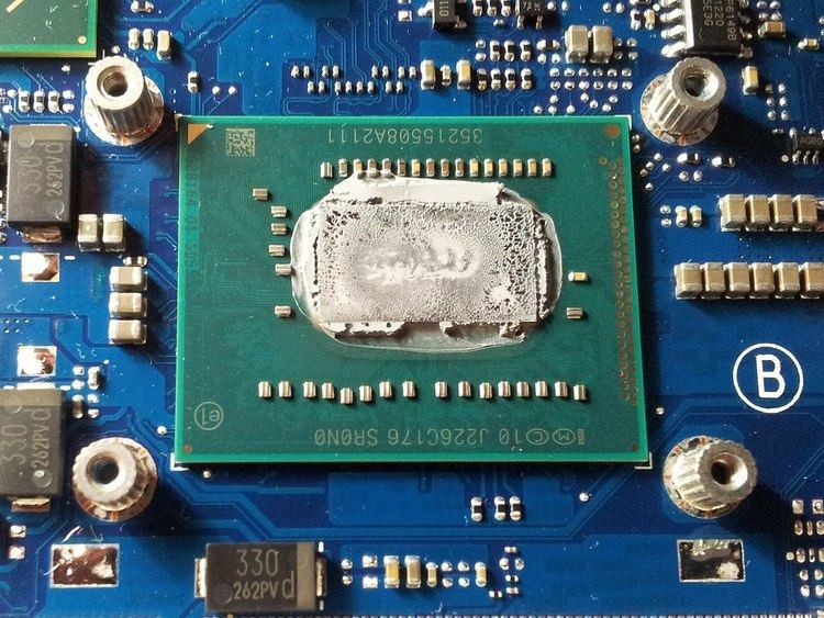
Ivy Bridge's temperatures are reportedly 10 °C higher compared to Sandy Bridge when a CPU is overclocked, even at default voltage setting. Impress PC Watch, a Japanese website, performed experiments that confirmed earlier speculations that this is because Intel used a poor quality (and perhaps lower cost) thermal interface material (thermal paste, or "TIM") between the chip and the heat spreader, instead of the fluxless solder of previous generations. The mobile Ivy Bridge processors are not affected by this issue because they do not use a heat spreader between the chip and cooling system.
Enthusiast reports describe the TIM used by Intel as low-quality, and not up to par for a "premium" CPU, with some speculation that this is by design to encourage sales of prior processors. Further analyses caution that the processor can be damaged or void its warranty if home users attempt to remedy the matter. The TIM has much lower thermal conductivity, causing heat to trap on the die. Experiments with replacing this TIM with a higher-quality one or other heat removal methods showed a substantial temperature drop, and improvements to the increased voltages and overclocking sustainable by Ivy Bridge chips.
Intel claims that the smaller die of Ivy Bridge and the related increase in thermal density is expected to result in higher temperatures when the CPU is overclocked; Intel also stated that this is as expected and will likely not improve in future revisions.
Models and steppings
All Ivy Bridge processors with one, two, or four cores report the same CPUID model 0x000306A9, and are built in four different configurations differing in the number of cores, L3 cache and GPU execution units.
Ivy Bridge-E/EN/EP/EX features
Ivy Bridge-E family is the follow-up to Sandy Bridge-E, using the same CPU core as the Ivy Bridge processor, but in LGA 2011, LGA 1356 and LGA 2011-1 packages for workstations and servers.
Models and steppings
The Ivy Bridge-E family is made in three different versions, by number of cores, and for three market segments: the basic Ivy Bridge-E is a single-socket processor sold as Core i7-49xx and is only available in the six-core S1 stepping, with some versions limited to four active cores.
Ivy Bridge-EN (Xeon E5-14xx v2 and Xeon E5-24xx v2) is the model for single- and dual-socket servers using LGA 1356 with up to 10 cores, while Ivy Bridge-EP (Xeon E5-16xx v2, Xeon E5-26xx v2 and Xeon E5-46xx v2) scales up to four LGA 2011 sockets and up to 12 cores per chip.
There are in fact three die "flavors" for the Ivy Bridge-EP, meaning that they are manufactured and organized differently, according to the number of cores an Ivy Bridge-EP CPU includes:
Ivy Bridge-EX has up to 15 cores and scales to 8 sockets. The 15-core die is organized into three columns of five cores, with three interconnect rings connecting two columns per ring; each five-core column has a separate L3 cache. The processor is supposed to have a new "Run Sure" technology, speculated by the odd number of cores to involve keeping one in reserve.
List of Ivy Bridge processors
Processors featuring Intel's HD 4000 graphics (or HD P4000 for Xeon) are set in bold. Other processors feature HD 2500 graphics unless indicated by N/A.
Desktop processors
List of announced desktop processors, as follows:
- Requires a compatible motherboard.
Suffixes to denote:
Server processors
Additional high-end server processors based on the Ivy Bridge architecture, code named Ivytown, were announced September 10, 2013 at the Intel Developer Forum, after the usual one year interval between consumer and server product releases.
The Ivy Bridge-EP processor line announced in September 2013 has up to 12 cores and 30 MB third level cache, with rumors of Ivy Bridge-EX up to 15 cores and an increased third level cache of up to 37.5 MB, although an early leaked lineup of Ivy Bridge-E included processors with a maximum of 6 cores.
Both Core-i7 and Xeon versions are produced: the Xeon versions marketed as Xeon E5-1400 V2 act as drop-in replacements for the existing Sandy Bridge-EN based Xeon E5, Xeon E5-2600 V2 versions act as drop-in replacements for the existing Sandy Bridge-EP based Xeon E5, while Core-i7 versions designated i7-4820K, i7-4930K and i7-4960X were released on 10 September 2013, remaining compatible with the X79 and LGA 2011 hardware.
For the intermediate LGA 1356 socket, Intel launched the Xeon E5-2400 V2 (codenamed Ivy Bridge-EN) series in January 2014. These have up to 10 cores.
A new Ivy Bridge-EX line marketed as Xeon E7 V2 had no corresponding predecessor using the Sandy Bridge microarchitecture but instead followed the older Westmere-EX processors.
- Requires a compatible motherboard.
Mobile processors
Suffixes to denote:
Roadmap
Intel demonstrated the Haswell architecture in September 2011, which began release in 2013 as the successor to Sandy Bridge and Ivy Bridge.