
Produced 2008 Max. CPU clock rate 4.4 GHz Instruction set z/Architecture | Min. feature size 65 nm Cores 4 | |
 | ||
The z10 is a microprocessor chip made by IBM for their System z10 mainframe computers, released February 26, 2008. It was called "z6" during development.
Contents
Description
The processor implements the CISC z/Architecture and has four cores. Each core has a 64 KB L1 instruction cache, a 128 KB L1 data cache and a 3 MB L2 cache (called the L1.5 cache by IBM). Finally, there is a 24 MB shared L3 cache (referred to as the L2 cache by IBM).
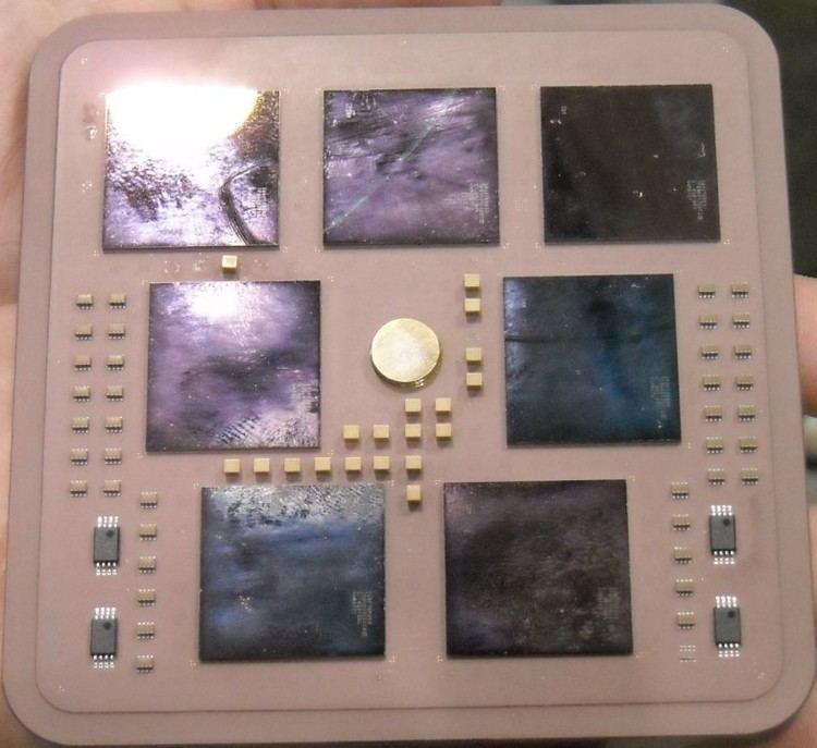
The chip measures 21.7×20.0 mm and consists of 993 million transistors fabricated in IBM's 65 nm SOI fabrication process (CMOS 11S), supporting speeds of 4.4 GHz and above – more than twice the clock speed as former mainframes – with a 15 FO4 cycle.
Each z10 chip has two 48 GB/s (48 billion bytes per second) SMP hub ports, four 13 GB/s memory ports, two 17 GB/s I/O ports, and 8765 contacts.
The z10 processor was co-developed with and shares many design traits with the POWER6 processor, such as fabrication technology, logic design, execution unit, floating-point units, bus technology (GX bus) and pipeline design style, i.e., a high frequency, low latency, deep (14 stages in the z10), in-order pipeline.
However, the processors are quite dissimilar in other respects, such as cache hierarchy and coherency, SMP topology and protocol, and chip organization. The different ISAs result in very different cores – there are 894 unique z10 instructions, 75% of which are implemented entirely in hardware. The z/Architecture is a CISC architecture, backwards compatible to the IBM System/360 architecture from the 1960s.
Additions to the z/Architecture from the previous z9 EC processor include:
Error detection and recovery is emphasized, with error-correcting code (ECC) on L2 and L3 caches and buffers, and extensive parity checking elsewhere; in all over 20,000 error checkers on the chip. Processor state is buffered in a way that allows precise core retry for almost all hardware errors.
Storage Control
Even though the z10 processor has on-die facilities for symmetric multiprocessing (SMP), there is a dedicated companion chip called the SMP Hub Chip or Storage Control (SC) that adds 24 MB off-die L3 cache and lets it communicate with other z10 processors and Hub Chips at 48 GB/s. The Hub Chip consists of 1.6 billion transistors and measures 20.8×21.4 mm, with 7984 interconnects. The design allows each processor to share cache across two Hub Chips, for a potential total of 48 MB of shared L3 cache.
Multi-chip module
On the System z10 Enterprise Class (EC) the z10 processors and the Storage Control (SC) chips are mounted on multi-chip modules (MCMs). Each z10 EC system can have up to four MCMs. One MCM consists of five z10 processors and two SC chips, totaling in seven chips per MCM. Due to redundancy, manufacturing issues, and other operating features, not all cores are available to the customer. The System z10 EC models E12, E26, E40 and E56, the MCMs have 17 available cores (one, two, three and four MCMs respectively), and the model E64 have one MCM with 17 cores, and three with 20 cores.