
 | ||
High energy X-ray imaging technology (HEXITEC) is a family of spectroscopic, single photon counting, pixel detectors developed for high energy X-ray and Ύ-ray spectroscopy applications.
Contents
- High energy X ray imaging technology
- The HEXITEC ASIC
- The PIXIE ASIC
- HEXITEC detectors
- Applications
- References
The HEXITEC consortium was formed in 2006 funded by the Engineering and Physical Sciences Research Council, UK. The consortium is led by the University of Manchester; other members include the Science and Technology Facilities Council, the University of Surrey, Durham University and University of London, Birkbeck. In 2010 the consortium expanded to include the Royal Surrey County Hospital and the University College London. The vision of the consortium was to "develop a UK-based capability in high energy X-ray imaging technology".
High energy X-ray imaging technology
X-ray spectroscopy is a powerful experimental technique that provides qualitative information about the elemental composition and internal stresses and strain within a specimen. High energy X-rays have the ability to penetrate deeply into materials allowing the examination of dense objects such as welds in steel, geological core sections bearing oil or gas or for the internal observation of chemical reactions inside heavy plant or machinery. Different experimental techniques such as X-ray fluorescence imaging and X-Ray diffraction imaging require X-ray detectors that are sensitive over a broad range of energies. Established semiconductor detector technology based on silicon and germanium have excellent energy resolution at X-ray energies under 30 keV but above this, due to a reduction in the material mass attenuation coefficient, the detection efficiency is dramatically reduced. To detect high energy X-rays, detectors produced from higher density materials are required.
High density, compound semiconductors such as cadmium telluride (CdTe), cadmium zinc telluride (CdZnTe), gallium arsenide (GaAs), mercuric iodide or thallium bromide have been the subject of extensive research for use in high energy X-ray detection. The favorable charge transport properties and high electrical resistivity of CdTe and CdZnTe have made them ideally suited to applications requiring spectroscopy at higher X-ray energies. Imaging applications, such as SPECT, require detectors with a pixelated electrode that allow objects to be imaged in 2D and 3D. Each pixel of the detector requires its own chain of readout electronics and for a highly pixelated detector this requires the use of a high sensitivity application-specific integrated circuit.
The HEXITEC ASIC
The HEXITEC application specific integrated circuit (ASIC) was developed for the consortium by the Science and Technology Facilities Council Rutherford Appleton Laboratory. The initial prototype consisted of an array of 20 x 20 pixels on a 250μm pitch fabricated using a 0.35μm CMOS process; the second generation of the ASIC expanded the array size to 80 x 80 pixels (4 cm2). Each ASIC pixel contains a charge amplifier, a CR-RC shaping amplifier and a peak track-and-hold circuit. The ASIC records the position and total charge deposited for each X-ray event detected.
The PIXIE ASIC
The PIXIE ASIC is a research and development ASIC developed by the Science and Technology Facilities Council Rutherford Appleton Laboratory for the consortium. The ASIC is being used to investigate charge induction and the small pixel effect in semiconductor detectors as described by the Shockley–Ramo theorem. The ASIC consists of three separate arrays of 3 x 3 pixels on a 250μm pitch and a single array of 3 x 3 pixels on a 500μm pitch. Each pixel contains a charge amplifier and output buffer allowing the induced charge pulses of each pixel to be recorded.
HEXITEC detectors
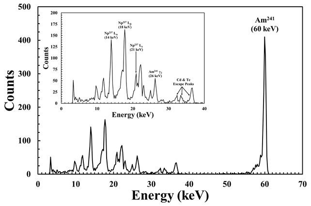
HEXITEC ASICs are flip-chip bonded to a direct conversion semiconductor detector using a low temperature (~100oC) curing silver epoxy and gold stud technique in a hybrid detector arrangement. The X-ray detector layer is a semiconductor, typically cadmium telluride (CdTe) or cadmium zinc telluride (CdZnTe), between 1 – 3 mm thick. The detectors consist of a planar cathode and a pixelated anode and are operated under a negative bias voltage. X-ray and Ύ-rays interacting within the detector layer form charge clouds of electron-hole pairs which drift from the cathode to the anode pixels. The charge drifting across the detectors induce charge on the ASIC pixels as described by the Shockley–Ramo theorem which form the detected signal. The detectors are capable of measuring an X-ray/Ύ-ray photo-peak FWHM of the order 1 keV in the energy range 3 - 200 keV.
Applications
HEXITEC detectors are in use in a number of different application areas including: materials science, medical imaging, illicit material detection, and X-ray astronomy,