65 nm G98 GPUPCI-E x1664 Bit Bus Width4 ROP, 8 Unified Shaders540 MHz Core Clock256 MB DDR2, 400 MHZ Memory Clock1300 MHZ Shader Clock5.1 G texels/s fill rate7.6 GB/s Memory bandwidthSupports DirectX 10, SM 4.0OpenGL 2.1 ComplianceSupports 1st generation PureVideo HD technology with partial VC1 decoding.On May 1, 2008 the GeForce 9300 GS was officially launched.
80 nm G86GPUPCI-E x1664 Bit Bus Width8 ROP, 16 Unified Shaders450 MHz Core Clock512 MB DDR2, 400 MHz Memory Clock900 MHz Shader Clock3.6 G texels/s fill rate6.4 GB/s Memory bandwidthSupports DirectX 10, SM 4.0OpenGL 2.1 ComplianceOn August 27, 2008 the GeForce 9400 GT was officially launched.
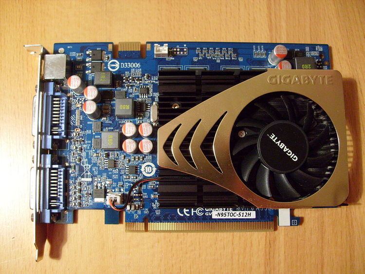
65 nm G96 GPU16 Stream Processors550 MHz core, with a 1350 MHz unified shader clock4.4 billion texels/s fillrate256 MB/512 MB/1024 MB 800 MHz DDR2 or 256 MB 1600 MHz GDDR3, both with a 128-bit memory bus12.8 GB/s memory bandwidth for boards configured with DDR2 800 MHz memorySupport DirectX 10, Shader Model 4.0, OpenGL 3.3, and PCI-Express 2.0Supports 2nd generation PureVideo HD technology with partial VC1 decoding and HybridPower technology.Minimum of 300 watt power supply supportedOn July 29, 2008 the GeForce 9500 GT was officially launched.
65 nm G96 GPU32 Stream Processors(32 Cuda Cores)4 Multi processor(each multi processor has 8 cores)550 MHz core, with a 1400 MHz unified shader clock.8.8 billion texels/s fillrate.256 MB/512 MB/1024 MB 1,600 MHz GDDR3 memory or 256 MB/512 MB 1,000 MHz GDDR2 memory, both with a 128-bit memory bus.25.6 GB/s memory bandwidth for boards configured with GDDR3 800 MHz memory.Support DirectX 10, Shader Model 4.0, OpenGL 3.3, and PCI-Express 2.0.Supports 2nd generation PureVideo HD technology with partial VC1 decoding.NVIDIA SLI - ready technologyHDMI supportThe 9500 GS is an OEM card that is based on the 9500 GT but geared towards the mainstream audience.
65 nm G96 GPU32 Stream Processors.8 Raster Operations (ROP) units550 MHz Core, with a 1375 MHz unified shader clock.8.8 billion texels/s Fillrate.128/512 MB 1000 MHz DDR2 memory with a 128-bit memory bus.16.0 GB/s memory bandwidth.Supports DirectX 10, Shader Model 4.0, OpenGL 3.3, and PCI-Express 2.0Supports 2nd generation PureVideo HD technology with partial VC1 decoding.NVIDIA SLI - ready technologyHDMI supportOn February 21, 2008, the GeForce 9600 GT was officially launched. It was an upgrade of 8600 GTS.
65 nm G94 GPU.64 stream processors.16 raster operation (ROP) units, 32 texture address (TA)/texture filter (TF) units.20.8 billion texels/s fill rate.650 MHz core clock, with a 1625 MHz unified shader clock.1008 MHz memory (2016 MHz datarate), 256-bit interface for 64.5GB/s of bandwidth. (57.6 GB/s for 1800 MHz configuration).512 MB - 2048 MB of GDDR3 or DDR2 memory.505M transistor countDirectX 10.0, Shader Model 4.0, OpenGL 2.1, and PCI-Express 2.0.Supports second-generation PureVideo HD technology with partial VC1 decoding.Is HDCP compatible, but its implementation depends on the manufacturer.Supports CUDA and the Quantum Effects physics processing engine.Almost double the performance of the previous Nvidia mid-range card, the GeForce 8600GTS.The GeForce 9600GS is a Hewlett Packard OEM card. It is based on a G94a core clocked at 500 MHz. It features 768 MB of DDR2 memory on a 192-bit bus o
The GeForce 9600 GSO was essentially a renamed 8800 GS. This tactic has been seen before in products such as the GeForce 7900 GTO to clear unsold stock when it is made obsolete by the next generation. Just like the 8800 GS, the 9600 GSO features 96 stream processors, a 550 MHz core clock with shaders clocked at 1,375 MHz, and either 384 or 768 MB of memory clocked at 800 MHz on a 192-bit memory bus. Some manufacturers have mistakenly listed some of their 768 MB models that have 96 stream processors as being based on the G94 chip, rather than the G92.
After clearing the old 8800 GS stock, Nvidia revised the specification with a new core, and 512 MB of memory clocked at 900 MHz on a 256-bit bus. For these cards, the number of stream processors is halved to 48, with the core frequency increased to 650 MHz and the shader frequency increased to 1625 MHz. Some of these cards have 1024 megabytes of memory while still being a 512 model. The revised version is considered inferior in performance to the old version.
XFX released a 9600 GTX based on the G92 chip featuring 96 stream processors, a 580 MHz core clock, 1450 MHz shaders and 512 MB of GDDR3 running at 1400 MHz on a 256-bit bus. Other than clock speeds, it is functionally the desktop equivalent version of the 9800M GT.
The GeForce 9800 series contains the GX2 (dual GPU), GTX, GTX+ and GT variants.
On March 18, 2008 the GeForce 9800 GX2 was officially launched.
The GeForce 9800 GX2 has the following specifications:.
Dual PCBs, dual GPU design197 W power consumption.Two 65nm process GPUs, with 256 total Stream Processors (128 per PCB).Supports Quad SLI.Power of Two underclocked GeForce 8800 GTS 512(G92) video cards in SLI Mode1 GiB (512 MiB per PCB) GDDR3 memory.Supports DirectX 10, Shader Model 4, OpenGL 3.3, and PCI-Express 2.0.Supports 2nd generation PureVideo HD technology with partial VC1 decoding.Outputs include two DVI ports, an HDMI output, and S/PDIF in connector on board for routing audio through the HDMI cable.An 8-pin and a 6-pin power connector.Clocks (Core/Shader/Memory): 600 MHz/1500 MHz/2000 MHz 256-bit memory interface128 GB/s memory bandwidthRelease date: March 18, 2008Launch price of $666.99.On April 1, 2008 the GeForce 9800 GTX was officially launched. It was basically an 8800 GTS 512MB with two SLI connectors, higher clock speeds, and support for Nvidia Hybrid Power, a technology that allows the discrete GPU to shut off during non resource intensive applications, and instead use the integrated GPU. With these extra features though, a high price came too.
Taken from an eVGA specification sheet:
128 Stream Processors.Clocks (Core/Shader/Memory): 675 MHz/1688 MHz/1100 MHz256-bit memory interface.512 MB of GDDR3 memory.70.4 GB/s memory bandwidthTexture Fill Rate of 43.2 (billion/s).DirectX 10, Shader Model 4.0, OpenGL 3.3, and PCI-Express 2.0.Supports 2nd generation PureVideo HD technology with partial VC1 decoding.Outputs include two DVI ports, an HDMI output(Using Nvidia DVI to HDMI adapter(included)), and S/PDIF in connector on board for routing audio through the HDMI cable.Release date was 2008-04-01.Launch Price of $349.In July 2008 Nvidia released a refresh of the 9800 GTX: the 9800 GTX+ (55 nm manufacturing process). It has faster core (738 MHz) and shader (1836 MHz) clocks. Since March 2009 this design is manufactured as GeForce GTS 250.
The 9800GT is identical to an 8800GT, although some were manufactured using a 55 nm technology instead of the 65 nm technology debuted on the 8800GT. The newer (55 nm) version supports HybridPower while the 65 nm version does not.
ASUSTeK have released a 9800GT with Tri-SLI support.
Taken from the Nvidia product detail page.
112 Stream Processors512-1024MB of GDDR3 memory256-bits Memory Interface Width600 MHz Graphics Clock1500 MHz Processor Clock900 MHz Memory ClockTexture Fill Rate (billion/s) 33.6Memory Bandwidth (GB/s) 57.6DirectX 10, Shader Model 4.0, OpenGL 3.3, and PCI-Express 2.0.Supports 2nd generation PureVideo HD technology with partial VC1 decoding.1 Unified shaders : Texture mapping units : Render output unitsCompute Capability: 1.1 has support for Atomic functions, which are used to write thread-safe programs.All graphical processing units in the GeForce 9M series feature:
Increased performance for similar power draw compared to GeForce 8M series for midrange and mid-high range notebooksDirectX 10.0 and OpenGL 3.3 compatibility16X antialiasing and PCI-Express 2.0 connectivityFull HD DVD / Blu-ray hardware decoding1 TMU per pipeline.4 ROPs.8 Stream Processors Cores.16 (v4.0) shader unified.26 Gigaflops.450 MHz core clock.1100 MHz shader clock.Integrated RAMDAC clock at 400 MHz.Memory Clock depend on System Memory.Up to 256 MB shared memory, 512 MB with Turbo Cache in Windows XP.64 bit memory interface (single-channel mode) / 128 bit memory interface (dual-channel mode).Memory Bandwidth depend on System Memory.1.8 billion texels/s texture fill rate.(Specification based on Acer Aspire 4530 using EVEREST Ultimate Edition Version 4.60.1500PX and TechPowerUp GPU-Z v0.4.6)8 Stream Processors.529 MHz core clock.1300 MHz shader clock.400 MHz memory clock.Up to 256 MB memory.64-bit memory interface.6.4 GB/s memory bandwidth.27.1GPixel/s pixel fill rate.4.2GTexel/s texture fill rate16 Stream Processors.400 MHz core clock.800 MHz shader clock.600 MHz memory clock.Up to 512 MB memory.64-bit memory interface.1.8 GB/s memory bandwidth.3.2 billion texels/s texture fill rate.8 Stream Processors.580 MHz core clock.1450 MHz shader clock.800 MHz memory clock.Up to 512 MB memory.64-bit memory interface.6.9 GB/s memory bandwidth.4.6 billion texels/s texture fill rate.16 Stream Processors.Memory Clock depend on System Memory.64 bit memory interface (single-channel mode) / 128 bit memory interface (dual-channel mode).Memory Bandwidth depends on System Memory.3.6 billion texels/s texture fill rate.16 Processors.500? billion texels/s texture fill rate.32 Stream Processors.475 MHz core clock.950 MHz shader clock.700 MHz memory clock.Up to 512 MB memory.128-bit memory interface.22.4 GB/s memory bandwidth.7.6 billion texels/s texture fill rate.064A/8 core (G96).32 Stream Processors.430 MHz core clock.1075 MHz shader clock.800/1600 MHz memory clock (effective).Up to 1024 MB memory.128-bit memory interface.12.8 GB/s (with DDR2 type) or 25.6 GB/s (with GDDR3 type) memory bandwidth.6.8 billion texels/s texture fill rate.103 GigaFLOPS.32 Stream Processors.500 MHz core clock.1250 MHz shader clock.1000 MHz memory clock.Up to 1024 MB memory.128-bit memory interface.25.6 GB/s memory bandwidth.8.0 billion texels/s texture fill rate.G96 core (65/55 nm).32 Stream Processors.550 MHz core clock.1325 MHz shader clock.800 MHz memory clock.Up to 1024 MB memory.128 bit memory interface.25.6 GB/s memory bandwidth.8.8 billion texels/s texture fill rate.G96 core.32 Stream Processors.625 MHz core clock.1550 MHz shader clock.800 MHz memory clock.128 bit memory interface.25.6 GB/s memory bandwidth.10.0 billion texels/s texture fill rate.148.8 GigaFLOPS.G94 core.48 Stream Processors.530 MHz core clock.1325 MHz shader clock.800 MHz memory clock.256 bit memory interface.51.2 GB/s memory bandwidth.12.7 billion texels/s texture fill rate.190.8 GigaFLOPS.G94 core.64 Stream Processors.530 MHz core clock.1325 MHz shader clock.800 MHz memory clock.256 bit memory interface.51.2 GB/s memory bandwidth.17.0 billion texels/s texture fill rate.254 GigaFLOPS.G94 core.64 Stream Processors.600 MHz core clock.1500 MHz shader clock.800 MHz memory clock.256 bit memory interface.51.2 GB/s memory bandwidth.19.2 billion texels/s texture fill rate.288 GigaFLOPS.G94 core.96 Stream Processors.500 MHz core clock.1250 MHz shader clock.800 MHz memory clock.256 bit memory interface.51.2 GB/s memory bandwidth.24.0 billion texels/s texture fill rate.360 GigaFLOPS.G92 core.112 Stream Processors.500 MHz core clock.1250 MHz shader clock.800 MHz memory clock.256 bit memory interface.51.2 GB/s memory bandwidth.28.0 billion texels/s texture fill rate.420 GigaFLOPS.NVIDIA has ceased driver support for GeForce 9 series on April 1, 2016.
Windows XP 32-bit & Media Center Edition: version 340.52 (WHQL) released on July 29, 2014; DownloadWindows XP 64-bit: version 340.52 (WHQL) released on July 29, 2014; DownloadWindows Vista, 7, 8, 8.1 32-bit: version 342.01 (WHQL) released on December 14, 2016; DownloadWindows Vista, 7, 8, 8.1 64-bit: version 342.01 (WHQL) released on December 14, 2016; DownloadWindows 10, 32-bit: version 342.01 (WHQL) released on December 14, 2016; DownloadWindows 10, 64-bit: version 342.01 (WHQL) released on December 14, 2016; Download