
Release date March 22, 2012 | Codename GK10x | |
 | ||
Models GeForce SeriesGeForce GT SeriesGeForce GTX Series Fabrication process and transistors 292M 40 nm (GF119)585M 40 nm (GF108)1.170M 40 nm (GF116)1.950M 40 nm (GF114)1.270M 28 nm (GK107)1.270M 28 nm (GK208)2.540M 28 nm (GK106)3.540M 28 nm (GK104) Entry-level GT 610GT 620GT 630GT 640 | ||
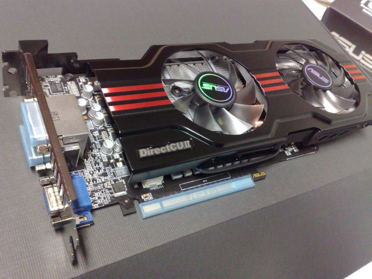
The GeForce 600 Series is a family of graphics processing units developed by Nvidia, used in desktop and laptop PCs. It serves as the introduction for the Kepler architecture (GK-codenamed chips), named after the German mathematician, astronomer, and astrologer Johannes Kepler. GeForce 600 series cards were first released in 2012.
Contents
Overview
Where the goal of the previous architecture, Fermi, was to increase raw performance (particularly for compute and tessellation), Nvidia's goal with the Kepler architecture was to increase performance per watt, while still striving for overall performance increases. The primary way Nvidia achieved this goal was through the use of a unified clock. By abandoning the shader clock found in their previous GPU designs, efficiency is increased, even though it requires more cores to achieve similar levels of performance. This is not only because the cores are more power efficient (two Kepler cores using about 90% of the power of one Fermi core, according to Nvidia's numbers), but also because the reduction in clock speed delivers a 50% reduction in power consumption in that area.
Kepler also introduced a new form of texture handling known as bindless textures. Previously, textures needed to be bound by the CPU to a particular slot in a fixed-size table before the GPU could reference them. This led to two limitations: one was that because the table was fixed in size, there could only be as many textures in use at one time as could fit in this table (128). The second was that the CPU was doing unnecessary work: it had to load each texture, and also bind each texture loaded in memory to a slot in the binding table. With bindless textures, both limitations are removed. The GPU can access any texture loaded into memory, increasing the number of available textures and removing the performance penalty of binding.
Finally, with Kepler, Nvidia was able to increase the memory clock to 6 GHz. To accomplish this, Nvidia needed to design an entirely new memory controller and bus. While still shy of the theoretical 7 GHz limitation of GDDR5, this is well above the 4 GHz speed of the memory controller for Fermi.
Architecture
The GeForce 600 Series contains products from both the older Fermi and newer Kepler generations of Nvidia GPUs. Kepler based members of the 600 series add the following standard features to the GeForce family:
Streaming Multiprocessor Architecture (SMX)
The Kepler architecture employs a new Streaming Multiprocessor Architecture called SMX. The SMX are the key method for Kepler's power efficiency as the whole GPU uses a single "Core Clock" rather than the double-pump "Shader Clock". The SMX usage of a single unified clock increases the GPU power efficiency due to the fact that two Kepler CUDA Cores consume 90% power of one Fermi CUDA Core. Consequently, the SMX needs additional processing units to execute a whole warp per cycle. Kepler also needed to increase raw GPU performance as to remain competitive. As a result, it doubled the CUDA Cores from 16 to 32 per CUDA array, 3 CUDA Cores Array to 6 CUDA Cores Array, 1 load/store and 1 SFU group to 2 load/store and 2 SFU group. The GPU processing resources are also double. From 2 warp schedulers to 4 warp schedulers, 4 dispatch unit became 8 and the register file doubled to 64K entries as to increase performance. With the doubling of GPU processing units and resources increasing the usage of die spaces, The capability of the PolyMorph Engine aren't double but enhanced, making it capable of spurring out a polygon in 2 cycles instead of 4. With Kepler, Nvidia not only worked on power efficiency but also on area efficiency. Therefore, Nvidia opted to use eight dedicated FP64 CUDA cores in a SMX as to save die space, while still offering FP64 capabilities since all Kepler CUDA cores are not FP64 capable. With the improvement Nvidia made on Kepler, the results include an increase in GPU graphic performance while downplaying FP64 performance.
A new instruction scheduler
Additional die areas are acquired by replacing the complex hardware scheduler with a simple software scheduler. With software scheduling, warps scheduling was moved to Nvidia's compiler and as the GPU math pipeline now has a fixed latency, it now include the utilization of instruction-level parallelism and superscalar execution in addition to thread-level parallelism. As instructions are statically scheduled, scheduling inside a warp becomes redundant since the latency of the math pipeline is already known. This resulted an increase in die area space and power efficiency.
GPU Boost
GPU Boost is a new feature which is roughly analogous to turbo boosting of a CPU. The GPU is always guaranteed to run at a minimum clock speed, referred to as the "base clock". This clock speed is set to the level which will ensure that the GPU stays within TDP specifications, even at maximum loads. When loads are lower, however, there is room for the clock speed to be increased without exceeding the TDP. In these scenarios, GPU Boost will gradually increase the clock speed in steps, until the GPU reaches a predefined power target (which is 170W by default). By taking this approach, the GPU will ramp its clock up or down dynamically, so that it is providing the maximum amount of speed possible while remaining within TDP specifications.
The power target, as well as the size of the clock increase steps that the GPU will take, are both adjustable via third-party utilities and provide a means of overclocking Kepler-based cards.
Microsoft DirectX support
Both Fermi and Kepler based cards support Direct3D 11. Kepler cards will also support Direct3D 12, though not all features provided by the API.
TXAA
Exclusive to Kepler GPUs, TXAA is a new anti-aliasing method from Nvidia that is designed for direct implementation into game engines. TXAA is based on the MSAA technique and custom resolve filters. Its design addresses a key problem in games known as shimmering or temporal aliasing; TXAA resolves that by smoothing out the scene in motion, making sure that any in-game scene is being cleared of any aliasing and shimmering.
NVENC
NVENC is Nvidia's SIP block that performs video encoding, in a way similar to Intel's Quick Sync Video and AMD's VCE. NVENC is a power-efficient fixed-function pipeline that is able to take codecs, decode, preprocess, and encode H.264-based content. NVENC specification input formats are limited to H.264 output. But still, NVENC, through its limited format, can perform encoding in resolutions up to 4096×4096.
Like Intel’s Quick Sync, NVENC is currently exposed through a proprietary API, though Nvidia does have plans to provide NVENC usage through CUDA.
New driver features
In the R300 drivers, released alongside the GTX 680, Nvidia introduced a new feature called Adaptive VSync. This feature is intended to combat the limitation of v-sync that, when the framerate drops below 60 FPS, there is stuttering as the v-sync rate is reduced to 30 FPS, then down to further factors of 60 if needed. However, when the framerate is below 60 FPS, there is no need for v-sync as the monitor will be able to display the frames as they are ready. To address this issue (while still maintaining the advantages of v-sync with respect to screen tearing), Adaptive VSync can be turned on in the driver control panel. It will enable VSync if the framerate is at or above 60 FPS, while disabling it if the framerate lowers. Nvidia claims that this will result in a smoother overall display.
While the feature debuted alongside the GTX 680, this feature is available to users of older Nvidia cards who install the updated drivers.
Dynamic Super Resolution (DSR) was added to Fermi and Kepler GPUs with an October 2014 release of Nvidia drivers. This feature aims at increasing the quality of displayed picture, by rendering the scenery at a higher and more detailed resolution, and scaling it down to match the monitor's native resolution.
History
In September 2010, Nvidia first announced Kepler.
In early 2012, details of the first members of the 600 series parts emerged. These initial members were entry-level laptop GPUs sourced from the older Fermi architecture.
On March 22, 2012, Nvidia unveiled the 600 series GPU: the GTX 680 for desktop PCs and the GeForce GT 640M, GT 650M, and GTX 660M for notebook/laptop PCs.
On April 29, 2012, the GTX 690 was announced as the first dual-GPU Kepler product.
On May 10, 2012, GTX 670 was officially announced.
On June 4, 2012, GTX 680M was officially announced.
On August 16, 2012, GTX 660 Ti was officially announced.
On September 13, 2012, GTX 660 and GTX 650 was officially announced.
On October 9, 2012, GTX 650 Ti was officially announced.
On March 26, 2013, GTX 650 Ti BOOST was officially announced.
GeForce 600 (6xx) series
GeForce 600M (6xxM) series
The GeForce 600M series for notebooks architecture. The processing power is obtained by multiplying shader clock speed, the number of cores and how many instructions the cores are capable of performing per cycle.