
 | ||
Embedded Wafer Level Ball Grid Array (eWLB) is a packaging technology for integrated circuits. The package interconnects are applied on an artificial wafer made of silicon chips and a casting compound.
Contents
eWLB is a further development of the classical Wafer Level Ball Grid Array Technology (WLB or WLP: wafer level package). The main driving force behind the eWLB technology was to allow fanout and more space for interconnect routing.
All process steps for the generation of the package are performed on the wafer. This allows, in comparison to classical packaging technologies (e. g. ball grid array), the generation of very small and flat packages with excellent electrical and thermal performance at lowest cost. It is common for all WLB technologies, which are built on a silicon wafer, that the interconnects (typically solder balls) fit on the chip (so called fan-in design). Therefore only chips with a restricted number of interconnects can be packaged.
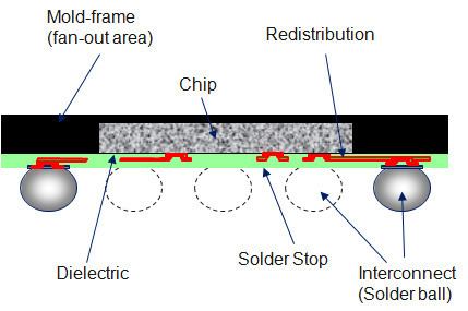
The eWLB technology allows the realization of chips with a high number of interconnects. The package is not created on a silicon wafer as for the classical Wafer Level Package, but on an artificial wafer. Therefore a front-end-processed wafer is diced and the singulated chips are placed on a carrier. The distance between the chips can be chosen freely, but it is typically larger than on the silicon wafer. The gaps and the edges around the chips are now filled with a casting compound to form a wafer. After curing an artificial wafer containing a mold frame around the dies for carrying additional interconnect elements is created. After the build of the artificial wafer (the so-called Reconstitution) the electrical connections from the chip pads to the interconnects are made in thin-film technology, as for any other classical Wafer Level Package.
With this technology any number of additional interconnects can be realized on the package in an arbitrary distance (fan-out design). Therefore, this Wafer Level Packaging Technology can also be used for space sensitive applications, where the chip area wouldn’t be sufficient to place the required number of interconnects at a suitable distance. The eWLB Technology was developed by Infineon, STMicroelectronics and STATS ChipPAC Ltd. First components were brought into market mid of 2009 (mobile phone).
Process Steps
- Lamination of foil onto carrier (Lamination tool)
- Chip placement onto wafer (Pick and place tool)
- Molding (Mold press)
- De-Bonding of carrier (de-bonding tool)
- Flip reconstructed wafer
- Ball drop reflow and wafer test