
 | ||
In electronics, diode modelling refers to the mathematical models used to approximate the actual behaviour of real diodes to enable calculations and circuit analysis. A diode's I-V curve is nonlinear (it is well described by the Shockley diode law). This nonlinearity complicates calculations in circuits involving diodes so simpler models are often required.
Contents
- Shockley diode model
- Diode resistor circuit example
- Explicit solution
- Iterative solution
- Graphical solution
- Piecewise linear model
- Mathematically idealized diode
- Ideal diode in series with voltage source
- Diode with voltage source and current limiting resistor
- Dual PWL diodes or 3 Line PWL model
- Resistance
- Capacitance
- Variation of Forward Voltage with Temperature
- References
This article discusses the modelling of p-n junction diodes, but the techniques may be generalized to other solid state diodes.
Shockley diode model
The Shockley diode equation relates the diode current
where
When
This expression is, however, only an approximation of a more complex I-V characteristic. Its applicability is particularly limited in case of ultrashallow junctions, for which better analytical models exist.
Diode-resistor circuit example
To illustrate the complications in using this law, consider the problem of finding the voltage across the diode in Figure 1.
Because the current flowing through the diode is the same as the current throughout the entire circuit, we can lay down another equation. By Kirchhoff's laws, the current flowing in the circuit is
These two equations determine the diode current and the diode voltage. To solve these two equations, we could substitute the current
Explicit solution
An explicit expression for the diode current can be obtained in terms of the Lambert W-function (also called the Omega function). A guide to these manipulations follows. A new variable
Following the substitutions
and
rearrangement of the diode law in terms of w becomes:
which using the Lambert
With the approximations (valid for the most common values of the parameters)
Once the current is determined, the diode voltage can be found using either of the other equations.
For large x,
Iterative solution
The diode voltage
By taking natural logarithms of both sides the exponential is removed, and the equation becomes
For any
or
The voltage of the source
Sometimes an iterative procedure depends critically on the first guess. In this example, almost any first guess will do, say
Graphical solution
Graphical analysis is a simple way to derive a numerical solution to the transcendental equations describing the diode. As with most graphical methods, it has the advantage of easy visualization. By plotting the I-V curves, it is possible to obtain an approximate solution to any arbitrary degree of accuracy. This process is the graphical equivalent of the two previous approaches, which are more amenable to computer implementation.
This method plots the two current-voltage equations on a graph and the point of intersection of the two curves satisfies both equations, giving the value of the current flowing through the circuit and the voltage across the diode. The figure illustrates such method.
Piecewise linear model
In practice, the graphical method is complicated and impractical for complex circuits. Another method of modelling a diode is called piecewise linear (PWL) modelling. In mathematics, this means taking a function and breaking it down into several linear segments. This method is used to approximate the diode characteristic curve as a series of linear segments. The real diode is modelled as 3 components in series: an ideal diode, a voltage source and a resistor.
The figure shows a real diode I-V curve being approximated by a two-segment piecewise linear model. Typically the sloped line segment would be chosen tangent to the diode curve at the Q-point. Then the slope of this line is given by the reciprocal of the small-signal resistance of the diode at the Q-point.
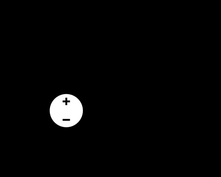
Mathematically idealized diode
Firstly, let us consider a mathematically idealized diode. In such an ideal diode, if the diode is reverse biased, the current flowing through it is zero. This ideal diode starts conducting at 0 V and for any positive voltage an infinite current flows and the diode acts like a short circuit. The I-V characteristics of an ideal diode are shown below:
Ideal diode in series with voltage source
Now let us consider the case when we add a voltage source in series with the diode in the form shown below:
When forward biased, the ideal diode is simply a short circuit and when reverse biased, an open circuit. If the anode of the diode is connected to 0 V, the voltage at the cathode will be at Vt and so the potential at the cathode will be greater than the potential at the anode and the diode will be reverse biased. In order to get the diode to conduct, the voltage at the anode will need to be taken to Vt. This circuit approximates the cut-in voltage present in real diodes. The combined I-V characteristic of this circuit is shown below:
The Shockley diode model can be used to predict the approximate value of
Using
Typical values of the saturation current at room temperature are:
As the variation of
For a current of 1.0 mA:
For a current of 100 mA:
Values of 0.6 or 0.7 volts are commonly used for silicon diodes
Diode with voltage source and current-limiting resistor
The last thing needed is a resistor to limit the current, as shown below:
The I-V characteristic of the final circuit looks like this:
The real diode now can be replaced with the combined ideal diode, voltage source and resistor and the circuit then is modelled using just linear elements. If the sloped-line segment is tangent to the real diode curve at the Q-point, this approximate circuit has the same small-signal circuit at the Q-point as the real diode.
Dual PWL-diodes or 3-Line PWL model
When more accuracy is desired in modelling the diode's turn-on characteristic, the model can be enhanced by doubling-up the standard PWL-model. This model uses two piecewise-linear diodes in parallel, as a way to model a single diode more accurately.
Resistance
Using the Shockley equation, the small-signal diode resistance
The latter approximation assumes that the bias current
Noting that the small-signal resistance
Capacitance
The charge in the diode carrying current
where
In a similar fashion as before, the diode capacitance is the change in diode charge with diode voltage:
where
Variation of Forward Voltage with Temperature
The Shockley diode equation has an exponential of
Here is some detailed experimental data, which shows this for a 1N4005 silicon diode. In fact, some silicon diodes are used as temperature sensors; for example, the CY7 series from OMEGA has a forward voltage of 1.02V in liquid nitrogen (77K), 0.54V at room temperature, and 0.29V at 100 °C.
In addition, there is a small change of the material parameter bandgap with temperature. For LEDs, this bandgap change also shifts their colour: they move towards the blue end of the spectrum when cooled.
Since the diode forward-voltage drops as its temperature rises, this can lead to thermal runaway in bipolar-transistor circuits (base-emitter junction of a BJT acts as a diode), where a change in bias leads to an increase in power-dissipation, which in turn changes the bias even further.