
 | ||
A digital timing diagram is a representation of a set of signals in the time domain. A timing diagram can contain many rows, usually one of them being the clock. It is a tool that is ubiquitous in digital electronics, hardware debugging, and digital communications. Besides providing an overall description of the timing relationships, the digital timing diagram can help find and diagnose digital logic hazards.
Contents
Diagram convention
Most timing diagrams use the following conventions:
Example: SPI bus timing
The timing diagram example on the right describes the Serial Peripheral Interface (SPI) Bus. Most SPI master nodes have the ability to set the clock polarity (CPOL) and clock phase (CPHA) with respect to the data. This timing diagram shows the clock for both values of CPOL and the values for the two data lines (MISO & MOSI) for each value of CPHA. Note that when CPHA=1 then the data is delayed by one-half clock cycle.
SPI operates in the following way:
When a slave's SS line is high then both of its MISO and MOSI line should be high impedance so to avoid disrupting a transfer to a different slave. Prior to SS being pulled low, the MISO & MOSI lines are indicated with a "z" for high impedance. Also, prior to the SS being pulled low the "cycle #" row is meaningless and is shown greyed-out.
Note that for CPHA=1 the MISO & MOSI lines are undefined until after the first clock edge and are also shown greyed-out before that.
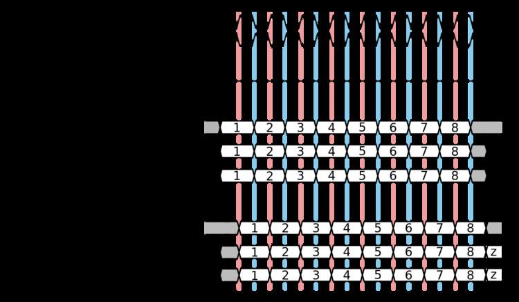
A more typical timing diagram has just a single clock and numerous data lines