
 | ||
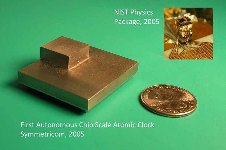
The Chip Scale Atomic Clock (CSAC) was a research program of the US Department of Defense's Defense Advanced Research Projects Agency (DARPA) to manufacture a microchip-sized atomic clock for use in portable equipment. In military equipment it is expected to provide improved location and battlespace situational awareness for dismounted soldiers when the global positioning system is not available, but many civilian applications are also envisioned. The program was initiated in 2001, and produced the first prototype cesium atomic clock chip in 2005. Commercial manufacturing of the chips began in 2011. The world's smallest atomic clock, the chip is 4 x 3.5 x 1 cm (1.5 x 1.4 x 0.4 inches) in size, weighs 35 grams, and consumes only 115 mW of power. It is accurate to 500 ns per day, or approximately one second in 5000 years.
Contents
How it works
Like other cesium clocks the chip keeps time with an ultraprecise 9.192631770 GHz microwave signal produced by electron transitions between two hyperfine energy levels in atoms of cesium 133, which is divided down by digital counters to give 10 MHz and 1 Hz clock signals provided to output pins. On the chip, liquid metal cesium in a tiny 2 mm capsule is heated to vaporize the cesium. A semiconductor laser shines a beam of infrared light modulated by a microwave oscillator through the capsule onto a photodetector. When the oscillator is at the precise frequency of the transition, the cesium atoms absorb the light, reducing the output of the photodetector. The output of the photodetector is used as feedback in a phase locked loop circuit to keep the oscillator at the correct frequency.
Development
Before the CSAC program, commercial cesium atomic clocks were bulky rack-mounted devices about the size of a suitcase weighing 30 kg, consuming about 100 W power and costing $70,000. Shrinking these to the size of a semiconductor chip required extensive development and several breakthroughs. An important part of development was designing the device so it could be manufactured using standard semiconductor fabrication techniques where possible, to keep its cost low enough that it could become a mass market device. Conventional cesium clocks use a glass cesium tube, which can't be made much smaller than 1 cm. In the CSAC, MEMS techniques were used to create a cesium capsule only 2 cubic millimeters in size. The light source in conventional atomic clocks is a rubidium atomic-vapor discharge lamp, which was bulky and consumed large amounts of power. In the CSAC this was replaced by an infrared vertical cavity surface emitting laser (VCSEL) fabricated on the chip, with its beam radiating upward into the cesium capsule above it.
However the largest barrier to miniaturization was the microwave cavity used in conventional clocks, whose size, equal to a wavelength of the microwave frequency, about 3 cm, formed the fundamental lower limit to the size of the clock. The breakthrough which solved this problem was the use of a quantum technique, coherent population trapping, which allowed the clock to do without a microwave cavity.