Rahul Sharma (Editor)

Charge pump

Updated on
Edit
Like
Comment
Share on FacebookTweet on TwitterShare on LinkedInShare on Reddit
Charge pump

A charge pump is a kind of DC to DC converter that uses capacitors as energy-storage elements to create either a higher- or lower-voltage power source. Charge-pump circuits are capable of high efficiencies, sometimes as high as 90–95%, while being electrically simple circuits.

Contents

Description

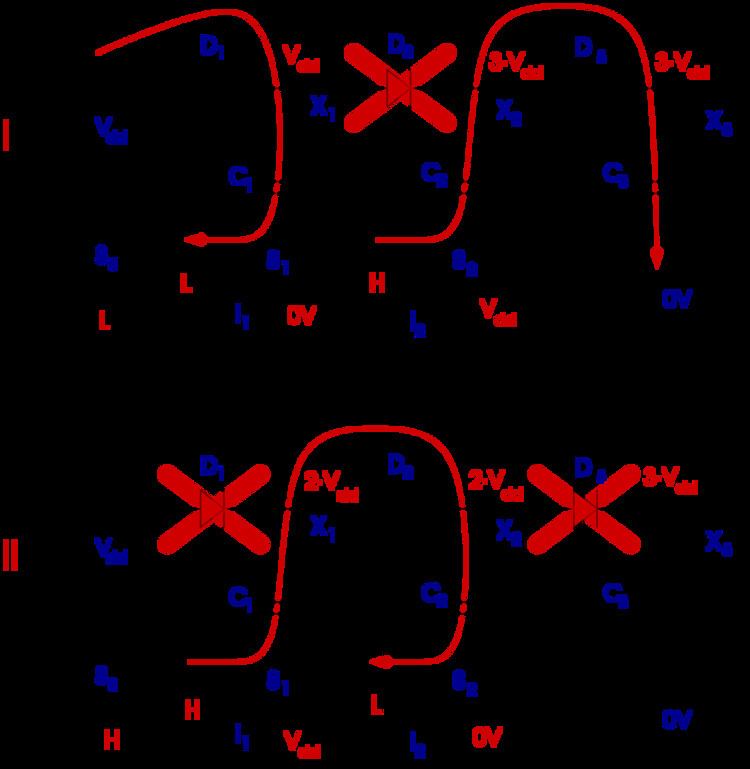
Charge pumps use some form of switching device(s) to control the connection of voltages to the capacitor. For instance, a two-stage cycle can be used to generate a higher pulsed voltage from a lower-voltage supply. In the first stage of the cycle, a capacitor is connected across the supply, charging it to that same voltage. In the second stage of the cycle, the circuit is reconfigured so that the capacitor is in series with the supply to the load. Ignoring leakage effects, this effectively provides double the supply voltage to the load (the sum of the original supply and the capacitor). The pulsing nature of the higher-voltage output is typically smoothed by the use of an output capacitor.

An external or secondary circuit drives the switching, typically at tens of kilohertz up to several megahertz. The high frequency minimizes the amount of capacitance required, as less charge needs to be stored and dumped in a shorter cycle. The capacitor used as the charge pump is typically known as the "flying capacitor".

Another way to explain the operation of a charge pump is to consider it as the combination of a DC to AC converter (the switches) followed by a voltage multiplier.

The voltage is load-dependent, and higher loads result in lower average voltages.

Charge pumps can double voltages, triple voltages, halve voltages, invert voltages, fractionally multiply or scale voltages (such as ×3/2, ×4/3, ×2/3, etc.) and generate arbitrary voltages by quickly alternating between modes, depending on the controller and circuit topology.

Terminology for PLL

The term charge pump is also commonly used in phase-locked loop (PLL) circuits even though there is no pumping action involved unlike in the circuit discussed above. A PLL charge pump is merely a bipolar switched current source. This means that it can output positive and negative current pulses into the loop filter of the PLL. It cannot produce higher or lower voltages than its power and ground supply levels.

Applications

  • A common application for charge-pump circuits is in RS-232 level shifters, where they are used to derive positive and negative voltages (often +10 V and −10 V) from a single 5 V or 3 V power supply rail.
  • Charge pumps can also be used as LCD or white-LED drivers, generating high bias voltages from a single low-voltage supply, such as a battery.
  • Charge pumps are extensively used in NMOS memories and microprocessors to generate a negative voltage "VBB" (about −3 V), which is connected to the substrate. This guarantees that all N+-to-substrate junctions are reversely biased by 3 V or more, decreasing junction capacitance and increasing circuit speed.
  • A charge pump providing a negative voltage spike has been used in NES-compatible games not licensed by Nintendo in order to stun the Nintendo Entertainment System lockout chip.
  • As of 2007, charge pumps are integrated into nearly all EEPROM and flash-memory integrated circuits. These devices require a high-voltage pulse to "clean out" any existing data in a particular memory cell before it can be written with a new value. Early EEPROM and flash-memory devices required two power supplies: +5 V (for reading) and +12 V (for erasing). As of 2007, commercially available flash memory and EEPROM memory requires only one external power supply – generally 1.8 V or 3.3 V. A higher voltage, used to erase cells, is generated internally by an on-chip charge pump.
  • Charge pumps are used in H bridges in high-side drivers for gate-driving high-side n-channel power MOSFETs and IGBTs. When the centre of a half bridge goes low, the capacitor is charged through a diode, and this charge is used to later drive the gate of the high-side FET a few volts above the source voltage so as to switch it on. This strategy works well, provided the bridge is regularly switched and avoids the complexity of having to run a separate power supply and permits the more efficient n-channel devices to be used for both switches. This circuit (requiring the periodic switching of the high-side FET) may also be called a "bootstrap" circuit, and some would differentiate between that and a charge pump (which would not require that switching).
  • References

    Charge pump Wikipedia