
 | ||
Chalcogenide chemical vapour deposition is a proposed technology for depositing thin films of chalcogenides, i.e. materials derived from sulfides, selenides, and tellurides. Conventional CVD can be used to deposit films of most metals, many non-metallic elements (notably silicon) as well as a large number of compounds including carbides, nitrides, oxides. CVD can be used to synthesize chalcogenide glasses.
Contents
Sulfide based thin films
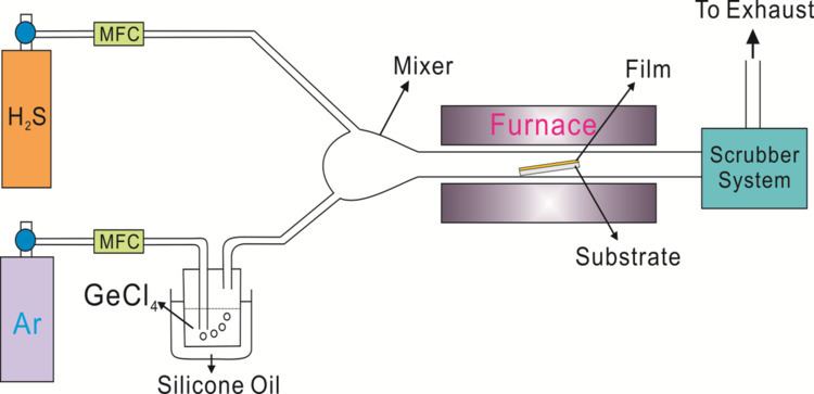
The fabrication of chalcogenide thin films is a topic of research. For example, routes to germanium disulfide films could entail germanium chloride and hydrogen sulphide:
GeCl4 (g) + 2 H2S(g) → GeS2(s) + 4 HCl (g)Alternatively via plasma enhanced CVD there is the reaction GeH4/H2S.
Telluride based thin films
Phase change random access memory (PCRAM) has attracted considerable interest as a candidate for non-volatile devices for higher density and operation speed. The ternary Ge2Sb2Te5 (GST) compound is widely regarded as the most viable and practical phase change family of materials for this application. CVD techniques have been applied to deposit GST materials in sub micron cell pores. Challenges include the need to control device to device variability and undesirable changes in the phase change material that can be induced by the fabrication procedure. A confined cell structure where the phase change material is formed inside a contact via is expected to be essential for the next generation PCRAM device because it requires lower switching power. This structure however requires more complex deposition of the active chalcogenide into a cell pore. CVD techniques could provide better performance and enable the production of thin films with superior quality compared to those obtained by sputtering, especially in terms of conformality, coverage, and stoichiometry control, and allows implementation of phase-change films in nanoelectronic devices. In addition, CVD deposition is well known to provide higher purity materials and provides the scope for new phase change materials with optimized properties to be deposited.
The CVD apparatus for Ge-Sb-Te thin film deposition is shown schematically to the right.