
 | ||
The CVAX is a microprocessor chip set developed and fabricated by Digital Equipment Corporation (DEC) that implemented the VAX instruction set architecture (ISA). The chip set consisted of the CVAX 78034 CPU, CFPA floating-point accelerator, CVAX clock chip, and the associated support chips, the CVAX System Support Chip (CSSC), CVAX Memory Controller (CMCTL), and CVAX Q-Bus Interface Chip (CQBIC).
Contents
CVAX 78034
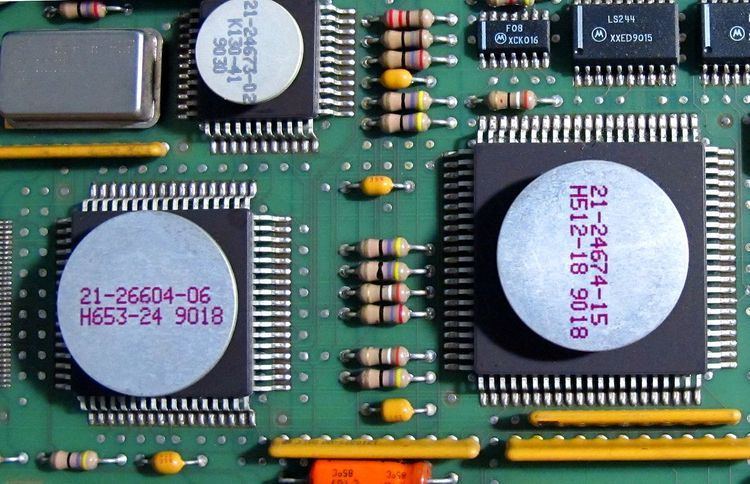
The CVAX 78034, also known as the MicroVAX 78034, is a second-generation single-chip VAX microprocessor. Systems featuring the CVAX chip set became available in late 1987. It is clocked at frequencies of 12.5 MHz (80 ns) in higher-end systems such as the VAX 6000 Model 200 and at 11.11 MHz (90 ns) in lower-end systems such as the MicroVAX 3500 and 3600.
The 78034 was the first VAX microprocessor to have internal caches, a 1 KB combined instruction and data stream cache. The cache is quite unusual as it is implemented with one-transistor DRAM, whereas the majority of microprocessors use SRAM for their internal caches. This was the first microprocessor to use one-transistor DRAM for cache. DEC chose to use DRAM for the cache to reduce the area of the cache array. The designers concluded that to implement this cache with four-transistor DRAM cells or six-transistor SRAM cells would have taken 2.4 to 3 times more area. The internal cache is located in a narrow strip along the left side of the die. An external 64 KB cache complements the 1 KB internal cache.
The 78034 contains 134,000 transistors on a die measuring 9.7 by 7.4 mm (71.78 mm2). It is fabricated in DEC's first-generation CMOS process, CMOS-1, a 2.0 µm CMOS process with two layers of aluminium interconnect. The 78034 is packaged in an 84-pin ceramic chip carrier with a heat sink. It uses single +5 volt power supply and dissipates a maximum of 1.5 W.
The microprocessor is microprogrammed and partially pipelined and consists of six major functional units, the I-Box, E-Box, M-box, bus interface unit (BIU), cache, and control store and microsequencer. The I-Box fetches VAX instructions from the cache and decodes them (parses) into macroinstructions. The I-Box has an IROM (Instruction decode ROM) that holds the information required to do so.
The E-Box consists of a register file, a 32-bit program counter, a constant generator, a shifter and an arithmetic logic unit (ALU). The register file contains 31 single-read-port/single-write-port registers and eight dual-read-port/single-write port registers. The ALU is 32-bit and is capable of executing addition, subtraction and logic instructions. Although the E-Box contains a dedicated shifter, the ALU also features a shifter, a less powerful one, for the purpose of executing integer multiply and divide instructions. The design of the register file permits these execution units to achieve higher performance by permitting more instances of simultaneous access to the registers.
The M-Box is the memory management unit. It has a 28-entry fully associative translation look-aside buffer (TLB) to translate virtual addresses into physical address. In addition to the TLB, it has registers that determine the memory address to read or write to. The M-Box works closely with the BIU, which controls access to the internal cache and interfaces the microprocessor to the 32-bit address data multiplexed external bus.
The control store and microsequencer provides the means of controls of the operation of the other functional units with microcode. The control store has a ROM containing 1,600 41-bit words. Each 41-bit word is divided into two, a 28-bit field that controls the functional units, and a 13-bit field that controls the microsequencer. Unlike the MicroVAX 78032, which uses X-shaped cells, the 78034 uses conventional H-shaped cells. The microsequencer's purpose is to supply microaddresses to the control store.
CFPA
The CFPA (CVAX Floating Point Accelerator) is a floating point coprocessor for the CVAX 78034.
The CFPA contains 65,000 transistors on a die measuring 7.3 by 9.1 mm (66.43 mm2). It is fabricated in DEC's first-generation CMOS process, CMOS-1, a 2.0 µm process with two layers of aluminium interconnect. It is packaged in a 68-pin surface mountable chip carrier.
CVAX+
CVAX+ referred to an optical shrink of the original CVAX fabricated in DEC's second-generation CMOS process, CMOS-2, a 1.5 µm process with two levels of wiring. The original design team shrunk the CVAX 78034, CFPA and CMCTL, with the other chips left unchanged. The shrunk 78034 was known as the CVAX-60, which taped out in August 1987, before the original 78034 begun volume production, and the CFPA-60 taped out in November 1987. The CVAX+ operated at 16.67 MHz, but power requirements was unchanged.
The CVAX+ started to ship in late 1988, as upgrades to all entry-level CVAX-based systems and were also provided as an upgrade to the VAX 6000 when the introduction of Rigel was delayed by yield issues.
SOC
SOC referred to a microprocessor which contained the CVAX 78034, CFPA, clock chip, and an 8 KB second level cache on a single die. Operating at 25 or 28.5 MHz, it was introduced in 1990 and used in entry-level servers, workstations, VXT-2000 X terminals, and as an embedded microprocessor in DEC's high-end printers and terminals. It was fabricated in DEC's third-generation CMOS process, CMOS-3, a 1.0 µm process with three levels of wiring.