
 | ||
The buck–boost converter is a type of DC-to-DC converter that has an output voltage magnitude that is either greater than or less than the input voltage magnitude. It is equivalent to a flyback converter using a single inductor instead of a transformer.
Contents
- Principle of operation of the 4 switch topology
- Principle of operation of the inverting topology
- Conceptual overview
- Continuous mode
- Discontinuous mode
- Limit between continuous and discontinuous modes
- Effect of parasitic resistances
- References
Two different topologies are called buck–boost converter. Both of them can produce a range of output voltages, ranging from much larger (in absolute magnitude) than the input voltage, down to almost zero.
Principle of operation of the 4-switch topology
The 4-switch converter combines the buck and boost converters. It can operate in either the buck or the boost mode. In either mode, only one switch controls the duty cycle, another is for commutation and must be operated inversely to the former one, and the remaining two switches are in a fixed position. A 2-switch buck-boost converter can be built with two diodes, but upgrading the diodes to FET transistor switches doesn't cost much extra while due to lower voltage drop the efficiency improves.
Principle of operation of the inverting topology
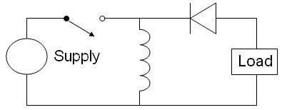
The basic principle of the inverting buck–boost converter is fairly simple (see figure 2):
Compared to the buck and boost converters, the characteristics of the inverting buck–boost converter are mainly:
Conceptual overview
Like the buck and boost converters, the operation of the buck-boost is best understood in terms of the inductor's "reluctance" to allow rapid change in current. From the initial state in which nothing is charged and the switch is open, the current through the inductor is zero. When the switch is first closed, the blocking diode prevents current from flowing into the right hand side of the circuit, so it must all flow through the inductor. However, since the inductor doesn't like rapid current change, it will initially keep the current low by dropping most of the voltage provided by the source. Over time, the inductor will allow the current to slowly increase by decreasing its voltage drop. Also during this time, the inductor will store energy in the form of a magnetic field.
Continuous mode
If the current through the inductor L never falls to zero during a commutation cycle, the converter is said to operate in continuous mode. The current and voltage waveforms in an ideal converter can be seen in Figure 3.
From
At the end of the On-state, the increase of IL is therefore:
D is the duty cycle. It represents the fraction of the commutation period T during which the switch is On. Therefore D ranges between 0 (S is never on) and 1 (S is always on).
During the Off-state, the switch S is open, so the inductor current flows through the load. If we assume zero voltage drop in the diode, and a capacitor large enough for its voltage to remain constant, the evolution of IL is:
Therefore, the variation of IL during the Off-period is:
As we consider that the converter operates in steady-state conditions, the amount of energy stored in each of its components has to be the same at the beginning and at the end of a commutation cycle. As the energy in an inductor is given by:
it is obvious that the value of IL at the end of the Off state must be the same with the value of IL at the beginning of the On-state, i.e. the sum of the variations of IL during the on and the off states must be zero:
Substituting
This can be written as:
This in return yields that:
From the above expression it can be seen that the polarity of the output voltage is always negative (because the duty cycle goes from 0 to 1), and that its absolute value increases with D, theoretically up to minus infinity when D approaches 1. Apart from the polarity, this converter is either step-up (a boost converter) or step-down (a buck converter). Thus it is named a buck–boost converter.
Discontinuous mode
In some cases, the amount of energy required by the load is small enough to be transferred in a time smaller than the whole commutation period. In this case, the current through the inductor falls to zero during part of the period. The only difference in the principle described above is that the inductor is completely discharged at the end of the commutation cycle (see waveforms in figure 4). Although slight, the difference has a strong effect on the output voltage equation. It can be calculated as follows:
Because the inductor current at the beginning of the cycle is zero, its maximum value
During the off-period, IL falls to zero after δ.T:
Using the two previous equations, δ is:
The load current
Replacing
Therefore, the output voltage gain can be written as:
Compared to the expression of the output voltage gain for the continuous mode, this expression is much more complicated. Furthermore, in discontinuous operation, the output voltage not only depends on the duty cycle, but also on the inductor value, the input voltage and the output current...
Limit between continuous and discontinuous modes
As told at the beginning of this section, the converter operates in discontinuous mode when low current is drawn by the load, and in continuous mode at higher load current levels. The limit between discontinuous and continuous modes is reached when the inductor current falls to zero exactly at the end of the commutation cycle. with the notations of figure 4, this corresponds to :
In this case, the output current
Replacing
As
Let's now introduce two more notations:
Using these notations, we have:
These expressions have been plotted in figure 5. The difference in behavior between the continuous and discontinuous modes can be seen clearly.
Effect of parasitic resistances
In the analysis above, no dissipative elements (resistors) have been considered. That means that the power is transmitted without losses from the input voltage source to the load. However, parasitic resistances exist in all circuits, due to the resistivity of the materials they are made from. Therefore, a fraction of the power managed by the converter is dissipated by these parasitic resistances.
For the sake of simplicity, we consider here that the inductor is the only non-ideal component, and that it is equivalent to an inductor and a resistor in series. This assumption is acceptable because an inductor is made of one long wound piece of wire, so it is likely to exhibit a non-negligible parasitic resistance (RL). Furthermore, current flows through the inductor both in the on and the off states.
Using the state-space averaging method, we can write:
where
When the switch is in the on-state,
The output current is the opposite of the inductor current during the off-state. the average inductor current is therefore:
Assuming the output current and voltage have negligible ripple, the load of the converter can be considered purely resistive. If R is the resistance of the load, the above expression becomes:
Using the previous equations, the input voltage becomes:
This can be written as:
If the inductor resistance is zero, the equation above becomes equal to the one of the ideal case. But when RL increases, the voltage gain of the converter decreases compared to the ideal case. Furthermore, the influence of RL increases with the duty cycle. This is summarized in figure 6.