
Name Alexander Coucoulas | ||
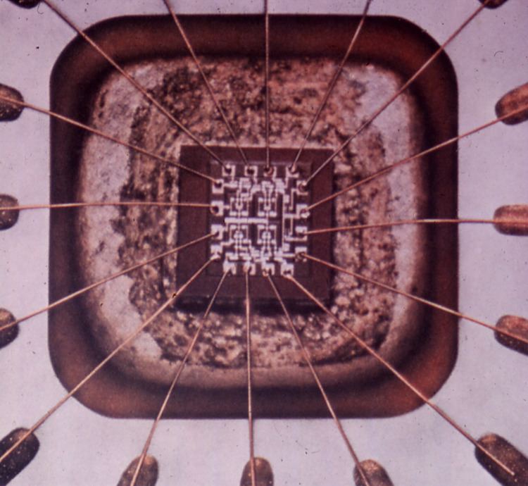 | ||
Alexander Coucoulas is an American inventor, research engineer, and author. He was named "Father Of Thermosonic Bonding" by George Harman, the world's foremost authority on wire bonding, where he referenced Coucoulas's leading edge publications in his book, Wire Bonding In Microelectronics. A Thermosonic bond is formed using a set of parameters which include ultrasonic, thermal and mechanical (force) energies. Figure 1 (below) shows a diagram of a Thermosonic Bonding machine which includes a magnetostrictive or piezoelectric-type transducer which is used to convert electrical energy into vibratory motion which is known as Piezoelectricity. The vibratory motion travels along the coupler system, a portion which is tapered to serve as the velocity transformer. The velocity transformer amplifies the oscilliatory motion and delivers it to a heated bonding tip.
Contents
- Personal background
- Thermosonic bonding
- Growing Applications Of Thermosonic Bonding
- Compliant bonding
- Extruding silica glass tubes for making optical fibers
- AlO bonding used to form a photonic switch
- Microstructure of Solid Carbon Dioxide Dry Ice
- Awards
- Some Publications And Presentations
- References
Thermosonic bonding is widely used to electrically connect silicon integrated circuit microprocessor chips into computers as well as a myriad of other electronic devices that require wire bonding.
As a result of Coucoulas introducing thermosonic bonding lead wires in the early 1960s, its applications and scientific investigations by researchers throughout the world have grown as confirmed by the thousands of Google search-sites. The all-important proven reliability of thermosonic bonding, as confirmed by these investigations, has made it the process of choice for connecting these crucially important electronic components. And since relatively low bonding parameters were shown to form reliable thermosonic bonds, the integrity of the fragile silicon integrated circuit chip central processor unit or CPU, is assured throughout its intended lifetime use as the "brains" of the computer.
Personal background
Coucoulas retired from AT&T Bell Labs as a member of the technical staff in 1996 where he pioneered research in the areas of electronic/photonics packaging, laser technology and optical fibers which resulted in numerous patents, and publications. He was twice awarded best paper which he presented at the 20th and 43rd IEEE Electronic Components Conference for “Compliant Bonding” in 1970 ” and AlO Bonding in 1993 both of which were his patented inventions.
His Ionian-Greek immigrant parents were born in the biblical city of Smyrna which was the birthplace of Homer. His single-parent father, Demetrios Koukoulas (as a maimed Smyrnaean Greek soldier), was rescued from the coastal waters of the Aegean sea by a Japanese naval cruiser while in view and during the devastating Fire of Smyrna in September 1922. The Japanese cruiser brought him to Pereaus, Greece where he immigrated to The United States via Ellis Island on the SS King Alexander in November of that same year.
Coucoulas, a native New Yorker (born 1933), served in the US Army as a combat engineer in the Far East Command in the early 1950s, and was awarded the National Defense Service Medal for the Korean War (1950-1954). He then obtained his undergraduate and graduate degrees in Metallurgical Engineering and Material Science at New York University which was financed by the GI Bill, a graduate scholarship and part-time jobs in the New York Metropolitan area. His graduate thesis was under the tutorage of Dr. Kurt Komarek, who is a former Rector (President) and present professor emeritus of the University Of Vienna. Coucoulas co-authored a paper with Dr. Komarek which included his thesis,. His spouse, Marie Janssen Coucoulas, played a significant supportive role throughout his professional career while also contributing to the welfare of learning disabled children in the capacity of a professional Learning Consultant. His daughters, Diane and Andrea, distinguished themselves as a University of North Carolina Professor and elementary student counselor respectively.
Thermosonic bonding
As mentioned above, in the mid 1960s, Alexander Coucoulas, reported the first thermosonic wire bonds using a combination of heat, ultrasonic vibrations and pressure which led to his first invention. He first set up a commercial ultrasonic wire bonder (capable of transmitting vibratory energy and pressure) in order to investigate the attachment of aluminum wires to tantalum thin films deposited on glass substrates which simulated bonding a lead wire to the fragile metallized silicon integrated circuit "chip". He observed that the ultrasonic energy and pressures levels needed to sufficiently deform the wire and form the required contact areas significantly increased the incidences of cracks in the glass or silicon chip substrates. A means of heating the bond region was then added to the ultrasonic bonder. The bond region was then heated during the ultrasonic bonding cycle which virtually eliminated the glass failure mode since the wire dramatically deformed to form the required contact area while using significantly lower ultrasonic energy and pressure levels. The enhanced wire deformation during the ultrasonic bonding cycle was attributed to the transition from cold working (or strain hardening of the wire) to near hot working conditions where its softness was enhanced. As the bonding temperature was increased the onset of recrystallization (softening mechanism) occurs where the strain hardening is most extensive. Thus the dual mechanisms of thermal softening and ultrasonic softening which is caused by vibratory energy interacting at the atomic lattice level, facilitated the desired wire deformation. Christian Hagar and George Harman stated that in 1970 Alexander Coucoulas reported additional work in forming thermosonic-type bonds which he initially called hot work ultrasonic bonding. In this case, copper wires were bonded to palladium thin films deposited on aluminum oxide substrates. As a result of these earliest reported thermosonic wire bonds, G.Harman stated "as such, Alexander Coucoulas is the Father of Thermosonic Bonding". At present, the majority of connections to silicon integrated circuits (the chip) are made using thermosonic bonding because it employs lower bonding temperatures, forces and dwell times than thermocompression bonding, as well as lower vibratory energy levels than ultrasonic bonding, to form the required bond area. As a result of using lower bonding parameters to form the required contact area, Thermosonic Bonding largely eliminates damaging the relatively fragile silicon integrated circuit micro-chip during the bonding cycle. The proven reliability of thermosonic bonding has made it the process of choice, since such potential failure modes could be costly whether they occur during the manufacturing stage or detected later, during an operational field-failure of a micro-chip which had been permanently connected inside a computer or a myriad of other electronic devices.
Another example showing the importance and reliability of using thermosonic bonding was when L Burmeister et al. of Hamburg University, Germany, reported that using solely ultrasonic power to bond gold wires to YBa2Cu3O7 microstructures, such as microbridges, Josephson junctions and superconducting interference devices (DC SQUIDS) can degrade them. Burmeister et al. stated that the problem was overcome by using Coucoulas’s thermosonic bonding process where it left the microstructure device intact so they could be employed.
Growing Applications Of Thermosonic Bonding
At present, the majority of connections to the silicon integrated circuit chip are made using thermosonic bonding because it employs lower bonding temperatures, forces and dwell times than thermocompression bonding, as well as lower vibratory energy levels and forces than ultrasonic bonding to form the required bond area. Therefore, the use of thermosonic bonding eliminates damaging the relatively fragile silicon integrated circuit chip during the bonding cycle. The proven reliability of thermosonic bonding has made it the process of choice, since such potential failure modes could be costly whether they occur during the manufacturing stage or detected later, during an operational field-failure of a chip which had been connected inside a computer or a myriad of other microelectronic devices.
Thermosonic bonding is also used in the flip chip process which is an alternate method of electrically connecting silicon integrated circuits.
Josephson effect and superconducting interference (DC SQUID) devices use the thermosonic bonding process as well. In this case, other bonding methods would degrade or even destroy YBaCuO₇ microstructures, such as microbridges, Josephson junctions and superconducting interference devices (DC SQUID).
When electrically connecting light-emitting diodes with thermosonic bonding techniques, an improved performance of the device has been shown.
Compliant bonding
Following his pioneering of thermosonic bonding, Coucoulas invents “Compliant Bonding which was a means of solid-state bonding the extended electroformed leads of a “beam leaded Chip” to the outside world. It was a unique method of solid state bonding in that the bonding energy (heat and pressure) was transmitted through a compliant aluminum tape. The compliant tape overcame the thickness variations of the beam leads and also acted as a chip carrier to the bonding site. In 1971, he was awarded best paper-presentation for “Compliant Bonding” which was among more than 90 papers presented at the 20th IEEE Electronic Components Conference in 1970 by engineers and research scientists from around the world.
Click pictures to enlarge view
Extruding silica glass tubes for making optical fibers
The first step in producing optical waveguides by the MCVD optical fiber process is making highly concentric fused silica tubes with a minimal variation along their entire length which translates into the critical ovality of the final optical fiber. Coucoulas proposed and reported the making of extruded fused silica tubes that closely followed the Poiseulle-Hagen equation for laminar flow and thus produced cladding tubes with dimensional properties required for making acceptable optical fibers. Coucoulas with collaborative colleagues was awarded patents regarding the tube making process.
AlO bonding used to form a photonic switch
Twenty-three years after being awarded best paper for “Compliant Bonding” as mentioned above, Coucoulas was again awarded Outstanding Paper at the 43rd Electronic Components and Technology Conference in 1993 (which he presented and co-authored with his collaborative colleagues).It was titled,"AlO Bonding: A Method of Joining Oxide Optical Components to Aluminum Coated Substrates." He also was awarded a U.S. patent for inventing AlO Bonding.
Microstructure of Solid Carbon Dioxide ("Dry Ice")
His first industrial research position was at Air Reduction Central Research facility in New Jersey where he investigated and co-authored a paper in the Transactions of the Metallurgical Society Of AIME entitled, “Some Observations on the Microstructure and Fragmentation of Solid Carbon Dioxide” with the following abstract:
Solid carbon dioxide (dry ice), which exists metastably as a constantly subliming molecular solid in a normal room temperature environment, was shown to exhibit many microstructural features which are similar to those observed in metals and ceramics at temperatures approaching their melting points. An investigation was made of factors affecting a costly brittleness condition known as "sandiness" which occurred in manufactured blocks of dry ice (polycrystalline solid carbon dioxide). The sandiness was found to be highly dependent on specific manufacturing and storage conditions that cause excessive grain growth which leads to a concentration of gas filled pores in the decreasing grain boundary regions.
Awards
Best paper and presentation for "Compliant Bonding" at the 20th Electronic Components Conference 1970 in Washington, D.C. (Awarded at the 21st Conference in 1971)
Certificate Of Appreciation For Advancing Microelectronics Technology, International Society For Hybrid Microelectronic (Indiana Chapter) 1971.
Outstanding paper and presentation for "AlO Bonding: A Method of Joining Oxide Optical Components to Aluminum Coated Substrates"at 43rd Electronic Components and Technology Conference in 1993.(Awarded at the 44th Conference in 1994)
Some Publications And Presentations
Physical Design Of Electronic Systems; co-authored Integrated Device And Connection Technology: Prentice-Hall Inc., Englewood Cliffs, New Jersey (1971)
Thin Film Technology; co-author; Robert E. Krieger Publication Company; Huntington N.Y. (1979)
Ultrasonic Welding of Aluminum Leads to Tantalum Thin Films, Transactions Metallurgical Society of AIME, 1966
Hot Work Ultrasonic Bonding – A Method Of Facilitating Metal Flow By Restoration Processes, Proceedings 20th IEEE Electronic Components Conf. Washington, D.C., May 1970,
Compliant Bonding, Proceedings 1970 IEEE 20th Electronic Components Conference, 1970.
“Extrusion Of Fused Silica Cladding Tubes For Making MCVD Optical Fibers, Third International Conference On Integrated Optics and Optical Fiber Communications, Technical Digest, San Francisco, Calif., April 1981.
AlO Bonding: A Method Of Joining Oxide Optical Components to Aluminum Coated Substrates (co-authored), Proceedings of the 43rd Electronic Components and Technology Conference, 1993.
Intra-company course for engineers entitled “Metallurgy Of Metal Bonding”.