
 | ||
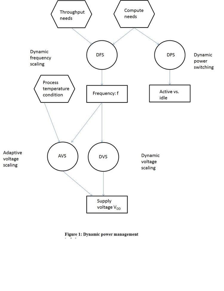
Adaptive Voltage Scaling (AVS) is a closed-loop dynamic power minimization technique that reduces power based on the actual operating conditions of the chip, i.e., the power consumption is continuously adjusted during the run time of the chip. Typically the design of any chip is done in such a way that it meets most demanding application throughput requirements under worst case operating conditions. This leads to an excess margin or wastage of power because the chip usually operates under typical operating conditions. AVS is beneficial compared to the conventional Dynamic voltage scaling (DVS) approach, a commonly encountered open loop dynamic power minimization technique, because AVS eliminates the excess power margins that are present in the open loop DVS systems due to the fixed voltage-frequency relations employed in those systems. In AVS technique the chip's exact process corner is determined either during the manufacturing test or during runtime and the appropriate Voltage-Frequency relationship is determined, which will be used during the dynamic voltage and frequency scaling operations. This eliminates the extra margin that will be present if the worst case operating conditions are taken into account while the chip is actually operating under typical conditions.
Contents
- Background
- Overview
- Comparison between the Open loop DVS technique and AVS
- Implementation of circuit that monitors On chip variations in the AVS systems
- Critical path monitoring techniques
- Challenges in Critical Path Monitoring Techniques
- Razor Approach
- Challenges in Razor approach
- Issues related to Bias Temperature InstabilityBTI
- References
Background
Technology scaling has enabled to design very powerful and versatile computing systems on smaller chips. As the smaller feature size allows more functions to be implemented in the same area, there is an escalation in current density and the associated power dissipation. As the demands for high processing power and clock-rates are ever increasing due to the higher integration, the power consumption and thermal performance of Integrated circuit is emerging as the limiting factor for high performance processor systems. Also the need for reducing the self-heating of the processor chips operating in automotive temperature environments enhances the need for solutions that reduce power dissipation .A lot of techniques can be used to transform a high-performance system into a low power system.However,minimizing power consumption in digital CMOS circuits requires a lot of design effort at system, architectural, circuit and device levels. Supply Voltage reduction technique is one of the most effective ways of reducing the power consumption.Nevertheless, one direct consequence of static supply voltage scaling is performance degradation.To maintain the desired throughput, Dynamic voltage scaling systems are used to adjust the supply voltage according to the throughput requirements . But there is still a large amount of power margin wasted in the Open-loop DVS systems and to overcome this AVS systems are being examined.
Overview
Adaptive voltage scaling is a closed-loop Dynamic voltage scaling approach that considers process variations from device to device on a chip,temperature fluctuations during the chip operations and load variations,and then establishes a voltage-frequency relation for the reduction in power dissipation of the circuit under that condition. The features offered by this approach are
The adaptive voltage Scaling technique is specifically used to address the energy saving requirements of Application-specific integrated circuit, Microprocessors or System on a chip. However AVS approach is ideally suited for high-volume systems such as Data centers and wireless base stations, as well as for the power constrained applications such as portable devices, USB peripherals, Consumer electronics.
Comparison between the Open loop DVS technique and AVS
The architecture of generic Dynamic Voltage Scaling system has a performance manager, a Phase-locked loop and a Voltage regulator. The performance manager block uses a software interface in order to predict the performance requirements of the next task.Once the determination of the power requirement is done, the voltage and frequency are set by the performance Manager in order to finish the task.The Phase-locked loop accomplishes the frequency scaling depending on the target frequency set by the performance manager.Similarly the Voltage regulator is programmed to scale the supply voltage so as to achieve the target voltage for the task.Thus, the characterization of the systems employing DVS requires characterization at at least two ends of operating range.In fact the characterization of DVS systems depends on the underlying voltage scaling methodology. The basic operation of both open loop DVS systems (the conventional DVS systems) and the closed loop DVS systems (Adaptive voltage systems) is same with the difference lying in the selection of the target voltage-frequency relationship. The Open-loop DVS systems employ the one-to-one mapping of the voltage to frequency to perform the voltage scaling.The frequency-voltage pairs are stored in Lookup table and are obtained as per the determined task needs.In case of the Open-loop DVS systems the frequency-voltage relationship is determined by considering the chip characterization at worst case conditions so as to guarantee the robust operation under the temperature and process variations.Thus in order to accommodate for the worst case variations there is a lot of power margin left by the open loop DVS systems for power scaling.This margin is not lost in closed loop systems because they employ a feedback mechanism that keeps probing the actual on chip conditions and according to that the target voltage and frequency are determined. The most important design parameters are to be considered while choosing between the Open-loop and closed loop configurations is stability against temperature fluctuations.The temperature stability is guaranteed in the conventional Open-loop systems because they are chosen for worst case conditions.But the energy savings are drastically reduced due to the large margins considered.
Implementation of circuit that monitors On-chip-variations in the AVS systems
The closed loop Voltage scaling system utilizes on chip circuit structures to provide feedback required to adaptively track the actual silicon behavior. One most commonly used approach is to use a ring oscillator that operates at the same voltage as that of the rest of the chip. The voltage-frequency relationship for the chip at that particular frequency is determined by the frequency of the ring oscillator.
Critical path monitoring techniques
The voltage-frequency relationship for the chip can also be determined by using another approach in which a critical path monitor tries to model the critical path of the chip.The critical path of the system can be duplicated using a ring oscillator or by a fanout of four Ring oscillator or a delay line. This critical path replica (delay line )provides the closest behavior to the actual critical path except for the intra-die variations and cross coupling capacitances which are hard to duplicate. This delay line adapts to environmental and process variations. As the actual performance of the core and the speed of the delay line are directly related, a closed-loop adaptive voltage scaling system is obtained to automatically adjust the supply voltage such that the minimum needed voltage is supplied so as to perform the target task. The delay chain consists of inverters, NAND gates, wire segments,etc., and the output can be tapped from one of the points, thus allowing tuning of the delay to match chips critical path. A reconfigurable delay chain can also be used in a critical path monitoring technique. It is during the manufacturing test, the exact setting of the delay chain is determined. During the AVS operation, in order to measure the delay launch an edge at the start of the clock cycle and then capture the edge at the end of the clock cycle at the output of delay chain and a set of buffers. Then the buffer outputs that are captured are analyzed to determine the exact positioning of the rising edge. Now the feedback employed by the AVS system continually adjusts the supply voltage such that the delay chain and critical path meet the timing constraints with adequate margins. The adjustment of supply voltage is done such that the launched rising edge makes it to a specified buffer stage which ensures the timing of delay line.
Challenges in Critical Path Monitoring Techniques
Sufficient safety margins are to be included in order to account for any mismatch between the delay line(critical path monitor) and the actual critical path in order to account for the large within-die process variations that are inevitable.These large variations can cause the critical path to change from one process corner to other.Thus in order to maintain a fail safe operation, an additional delay margin is to be maintained.This margin is translated into voltage overhead that directly reduces the energy savings associated with the AVS approach. The process and temperature variations of the closed loop systems are compensated by continuously monitoring the activity of critical path replica.Nevertheless, in the sub-micrometer technologies the use of a single reference in the critical path is becoming less feasible.As the transistor dimensions are scaled, selection of a unique critical path across all conditions becomes very challenging.This is because of the increased variations of transistor and wires with the progress of technology node.Also when the contribution of interconnect delay increases, there might be several paths that have different combinations of logic and interconnect delay with their overall delays being close to each other.In that case the selection of critical path becomes even more challenging.
Razor Approach
In order to overcome the bottlenecks of the Critical path approach implementation of AVS system, the Razor approach is used. Unlike the critical path approach where a single path is identified as critical path, Razor approach has a set of potential critical paths that are to be monitored. In this approach an on-chip timing checker is employed to check the timing margin of the set of critical path. A delayed version of the system clock is used by the timing circuit to capture the data in shadow latch which is same as the data captured by the master(main) flipflop. Wherever the sub paths become critical, additional shadow latches are introduced. When the supply voltage is scaled the value latched in the main flipflop might be different from that of those latched by the shadow latches, which results in an error signals. The error signals from all the shadow latches are gathered to generate a single error indicator. This error is corrected by flushing the pipeline and reloading the state that was existing before the error occurred. When the error rates decrease beyond certain limits the supply voltage is reduced till the point where the error tends to become unacceptable.
Challenges in Razor approach
Issues related to Bias Temperature Instability(BTI)
Bias temperature instability, an aging [sic?] mechanism in CMOS technology causes time dependent degradation in VLSI circuits. Adaptive voltage scaling can be used to mitigate the BTI-induced timing degradation by increasing the supply voltage dynamically. This can be achieved as long as the BTI degradation is captured by performance sensor in the AVS system. However the use of AVS during the lifetime of the chip poses new challenges for the margin reduction in the sign-off methodology which characterizes the timing libraries based on the transistor models with the pre-calculated BTI degradation for given integrated circuit life time.