
 | ||
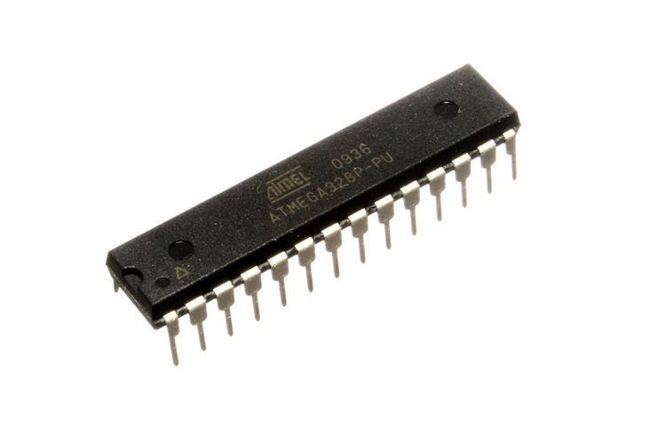
The ATmega328 is a single-chip microcontroller created by Atmel in the megaAVR family.
Contents
Specifications
The Atmel 8-bit AVR RISC-based microcontroller combines 32 kB ISP flash memory with read-while-write capabilities, 1 kB EEPROM, 2 kB SRAM, 23 general purpose I/O lines, 32 general purpose working registers, three flexible timer/counters with compare modes, internal and external interrupts, serial programmable USART, a byte-oriented 2-wire serial interface, SPI serial port, 6-channel 10-bit A/D converter (8-channels in TQFP and QFN/MLF packages), programmable watchdog timer with internal oscillator, and five software selectable power saving modes. The device operates between 1.8-5.5 volts. The device achieves throughput approaching 1 MIPS per MHz.
Series alternatives
A common alternative to the ATmega328 is the "picoPower" ATmega328P. A comprehensive list of all other member of the megaAVR series can be found on the Atmel website.
Applications
As of 2013 the ATmega328 is commonly used in many projects and autonomous systems where a simple, low-powered, low-cost micro-controller is needed. Perhaps the most common implementation of this chip is on the popular Arduino development platform, namely the Arduino Uno and Arduino Nano models.
Programming
Reliability qualification shows that the projected data retention failure rate is much less than 1 PPM over 20 years at 85 °C or 100 years at 25 °C.
Programming mode is entered when PAGEL (PD7), XA1 (PD6), XA0 (PD5), BS1 (PD4) is set to zero. RESET pin to 0V and VCC to 0V. VCC is set to 4.5 - 5.5V. Wait 60 μs, and RESET is set to 11.5 - 12.5 V. Wait more than 310 μs. Set XA1:XA0:BS1:DATA = 100 1000 0000, pulse XTAL1 for at least 150 ns, pulse WR to zero. This starts the Chip Erase. Wait until RDY/BSY (PD1) goes high. XA1:XA0:BS1:DATA = 100 0001 0000, XTAL1 pulse, pulse WR to zero. This is the Flash write command. And so on..
Serial data to the MCU is clocked on the rising edge and data from the MCU is clocked on the falling edge. Power is applied to VCC while RESET and SCK are set to zero. Wait for at least 20 ms and then the Programming Enable serial instruction 0xAC, 0x53, 0x00, 0x00 is sent to the MOSI pin. The second byte (0x53) will be echoed back by the MCU.