
First production 1971 | ||
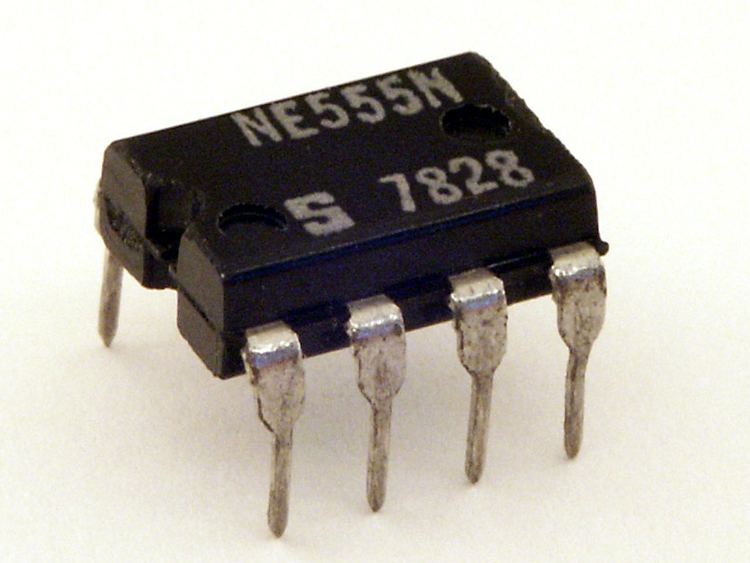 | ||
Type Active, Integrated circuit Pin configuration GND, TRIG, OUT, RESET, CTRL, THR, DIS, VCC | ||
The 555 timer IC is an integrated circuit (chip) used in a variety of timer, pulse generation, and oscillator applications. The 555 can be used to provide time delays, as an oscillator, and as a flip-flop element. Derivatives provide two or four timing circuits in one package.
Contents
- History
- Design
- Pins
- Modes
- Bistable
- Monostable
- Astable
- Specifications
- Packages
- Derivatives
- 556 dual timer
- 558 quad timer
- Joystick interface circuit using the 558 quad timer
- References
Introduced in 1972 by Signetics, the 555 is still in widespread use due to its low price, ease of use, and stability. It is now made by many companies in the original bipolar and in low-power CMOS. As of 2003, it was estimated that 1 billion units were manufactured every year. The 555 is the most popular integrated circuit ever manufactured.
History
The IC was designed in 1971 by Hans R. Camenzind under contract to Signetics (later acquired by Philips Semiconductors, and now NXP).
In 1962, Camenzind joined PR Mallory's Laboratory for Physical Science in Burlington, Massachusetts. He designed a pulse-width modulation (PWM) amplifier for audio applications, but it was not successful in the market because there was no power transistor included. He became interested in tuners such as a gyrator and a phase-locked loop (PLL). He was hired by Signetics develop a PLL IC in 1968. He designed an oscillator for PLLs such that the frequency did not depend on the power supply voltage or temperature. However, Signetics laid off half of its employees, and the development was frozen due to a recession.
Camenzind proposed the development of a universal circuit based on the oscillator for PLLs, and asked that he would develop it alone, borrowing their equipment instead of having his pay cut in half. Other engineers argued the product could be built from existing parts, but the marketing manager bought the idea. Among 5xx numbers that were assigned for analogue ICs, the special number "555" was chosen.
Camenzind also taught circuit design at his nearby university in the morning, and went to the Northeastern University to get the master's degree at night. The first design was reviewed in the summer of 1971. There was no problem, so it had gone to the layout design. A few days later, he got the idea of using a direct resistance instead of a constant current source, and found that it worked. The change decreased the required 9 pins to 8, so the IC could be fit in an 8-pin package instead of a 14-pin package. This design passed the second design review, and the prototype was completed in October 1971. Its 9-pin copy had been already released by another company founded by an engineer who attended the first review and retired from Signetics, but they withdrew it soon after the 555 was released. The 555 timer was manufactured by 12 companies in 1972 and it became the best selling product.
Design
Depending on the manufacturer, the standard 555 package includes 25 transistors, 2 diodes and 15 resistors on a silicon chip installed in an 8-pin mini dual-in-line package (DIP-8). Variants available include the 556 (a 14-pin DIP combining two 555s on one chip), and the two 558 & 559s (both a 16-pin DIP combining four slightly modified 555s with DIS & THR connected internally, and TR is falling edge sensitive instead of level sensitive).
The NE555 parts were commercial temperature range, 0 °C to +70 °C, and the SE555 part number designated the military temperature range, −55 °C to +125 °C. These were available in both high-reliability metal can (T package) and inexpensive epoxy plastic (V package) packages. Thus the full part numbers were NE555V, NE555T, SE555V, and SE555T. It has been hypothesized that the 555 got its name from the three 5 kΩ resistors used within, but Hans Camenzind has stated that the number was arbitrary.
Low-power versions of the 555 are also available, such as the 7555 and CMOS TLC555. The 7555 is designed to cause less supply noise than the classic 555 and the manufacturer claims that it usually does not require a "control" capacitor and in many cases does not require a decoupling capacitor on the power supply. Those parts should generally be included, however, because noise produced by the timer or variation in power supply voltage might interfere with other parts of a circuit or influence its threshold voltages.
Pins
The connection of the pins for a DIP package is as follows:
Pin 5 is also sometimes called the CONTROL VOLTAGE pin. By applying a voltage to the CONTROL VOLTAGE input one can alter the timing characteristics of the device. In most applications, the CONTROL VOLTAGE input is not used. It is usual to connect a 10 nF capacitor between pin 5 and 0 V to prevent interference. The CONTROL VOLTAGE input can be used to build an astable multivibrator with a frequency-modulated output.
Modes
The IC 555 has three operating modes:
- Bistable mode or Schmitt trigger – the 555 can operate as a flip-flop, if the DIS pin is not connected and no capacitor is used. Uses include bounce-free latched switches.
- Monostable mode – in this mode, the 555 functions as a "one-shot" pulse generator. Applications include timers, missing pulse detection, bounce-free switches, touch switches, frequency divider, capacitance measurement, pulse-width modulation (PWM) and so on.
- Astable (free-running) mode – the 555 can operate as an electronic oscillator. Uses include LED and lamp flashers, pulse generation, logic clocks, tone generation, security alarms, pulse position modulation and so on. The 555 can be used as a simple ADC, converting an analog value to a pulse length (e.g., selecting a thermistor as timing resistor allows the use of the 555 in a temperature sensor and the period of the output pulse is determined by the temperature). The use of a microprocessor-based circuit can then convert the pulse period to temperature, linearize it and even provide calibration means.
Bistable
In bistable (also called Schmitt trigger) mode, the 555 timer acts as a basic flip-flop. The trigger and reset inputs (pins 2 and 4 respectively on a 555) are held high via pull-up resistors while the threshold input (pin 6) is simply floating. Thus configured, pulling the trigger momentarily to ground acts as a 'set' and transitions the output pin (pin 3) to Vcc (high state). Pulling the reset input to ground acts as a 'reset' and transitions the output pin to ground (low state). No timing capacitors are required in a bistable configuration. Pin 5 (control voltage) is connected to ground via a small-value capacitor (usually 0.01 to 0.1 μF). Pin 7 (discharge) is left floating.
Monostable
The output pulse ends when the voltage on the capacitor equals 2/3 of the supply voltage. The output pulse width can be lengthened or shortened to the need of the specific application by adjusting the values of R and C.
The output pulse width of time t, which is the time it takes to charge C to 2/3 of the supply voltage, is given by
where t is in seconds, R is in ohms (resistance) and C is in farads (capacitance).
While using the timer IC in monostable mode, the main disadvantage is that the time span between any two triggering pulses must be greater than the RC time constant. Conversely, ignoring closely spaced pulses is done by setting the RC time constant to be larger than the span between spurious triggers. (Example: ignoring switch contact bouncing.)
Astable
In astable mode, the 555 timer puts out a continuous stream of rectangular pulses having a specified frequency. Resistor R1 is connected between VCC and the discharge pin (pin 7) and another resistor (R2) is connected between the discharge pin (pin 7), and the trigger (pin 2) and threshold (pin 6) pins that share a common node. Hence the capacitor is charged through R1 and R2, and discharged only through R2, since pin 7 has low impedance to ground during output low intervals of the cycle, therefore discharging the capacitor.
In the astable mode, the frequency of the pulse stream depends on the values of R1, R2 and C:
The high time from each pulse is given by:
and the low time from each pulse is given by:
where R1 and R2 are the values of the resistors in ohms and C is the value of the capacitor in farads.
The power capability of R1 must be greater than
Particularly with bipolar 555s, low values of
To have an output high time shorter than the low time (i.e., a duty cycle less than 50%) a small diode (that is fast enough for the application) can be placed in parallel with R2, with the cathode on the capacitor side. This bypasses R2 during the high part of the cycle so that the high interval depends only on R1 and C, with an adjustment based the voltage drop across the diode. The voltage drop across the diode slows charging on the capacitor so that the high time is a longer than the expected and often-cited ln(2)*R1C = 0.693 R1C. The low time will be the same as above, 0.693 R2C. With the bypass diode, the high time is
where Vdiode is when the diode's "on" current is 1/2 of Vcc/R1 which can be determined from its datasheet or by testing. As an extreme example, when Vcc= 5 and Vdiode= 0.7, high time = 1.00 R1C which is 45% longer than the "expected" 0.693 R1C. At the other extreme, when Vcc= 15 and Vdiode= 0.3, the high time = 0.725 R1C which is closer to the expected 0.693 R1C. The equation reduces to the expected 0.693 R1C if Vdiode= 0.
The operation of RESET in this mode is not well-defined. Some manufacturers' parts will hold the output state to what it was when RESET is taken low, others will send the output either high or low.
The astable configuration, with two resistors, cannot produce a 50% duty cycle. To produce a 50% duty cycle, eliminate R1, disconnect pin 7 and connect the supply end of R2 to pin 3, the output pin. This circuit is similar to using an inverter gate as an oscillator, but with fewer components than the astable configuration, and a much higher power output than a TTL or CMOS gate. The duty cycle for either the 555 or inverter-gate timer will not be precisely 50% and will change based off any load that the output is also driving while high (longer duty cycles for greater loads) due to the fact the timing network is supplied from the devices output pin, which has different internal resistances depending on whether it is in the high or low state (high side drivers tend to be more resistive).
Specifications
These specifications apply to the NE555. Other 555 timers can have different specifications depending on the grade (military, medical, etc.).
Packages
In 1972, Signetics originally released the 555 timer in 8-pin DIP and 8-pin TO-5 metal can packages, and the 556 timer was released in 14-pin DIP package.
Currently, the 555 is available in through-hole packages as DIP-8 and SIP-8 (both 2.54mm pitch), and surface-mount packages as SO-8 (1.27mm pitch), SSOP-8 / TSSOP-8 / VSSOP-8 (0.65mm pitch), BGA (0.5mm pitch). The Microchip/Micrel MIC1555 is a 555 CMOS timer with 3 fewer pins available in SOT23-5 (0.95mm pitch) surface mount package.
Derivatives
Many pin-compatible variants, including CMOS versions, have been built by various companies. Bigger packages also exist with two or four timers on the same chip. The 555 is also known under the following type numbers:
556 dual timer
The dual version is called 556. It features two complete 555s in a 14 pin DIL package.
558 quad timer
The quad version is called 558 and has 16 pins. To fit four 555s into a 16 pin package the power, control voltage, and reset lines are shared by all four modules. Each module's discharge and threshold circuits are wired together internally.
Joystick interface circuit using the 558 quad timer
The Apple II microcomputer used a quad timer 558 in monostable (or "one-shot") mode to interface up to four "game paddles" or two joysticks to the host computer. It also used a single 555 for flashing the display cursor.
A similar circuit was used in the IBM PC. In the joystick interface circuit of the IBM PC, the capacitor of the RC network (see Monostable Mode above) was generally a 10 nF capacitor. The resistor of the RC network consisted of the potentiometer inside the joystick along with an external resistor of 2.2 kΩ. The joystick potentiometer acted as a variable resistor. By moving the joystick, the resistance of the joystick increased from a small value up to about 100 kΩ. The joystick operated at 5 V.
Software running in the host computer started the process of determining the joystick position by writing to a special address (ISA bus I/O address 201h). This would result in a trigger signal to the quad timer, which would cause the capacitor of the RC network to begin charging and cause the quad timer to output a pulse. The width of the pulse was determined by how long it took the capacitor to charge up to 2/3 of 5 V (or about 3.33 V), which was in turn determined by the joystick position. The software then measured the pulse width to determine the joystick position. A wide pulse represented the full-right joystick position, for example, while a narrow pulse represented the full-left joystick position.