
 | ||
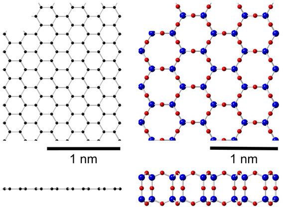
Two-dimensional silica (2D silica) is a layered polymorph of silicon dioxide. Two varieties of 2D silica, both of hexagonal crystal symmetry, have been grown so far on various metal substrates. One is based on SiO4 tetrahedra, which are covalently bonded to the substrate. The second comprises graphene-like fully saturated sheets, which interact with the substrate via weak van der Waals bonds. One sheet of the second 2D silica variety is also called hexagonal bilayer silica (HBS); it can have either ordered or disordered (amorphous) structure.
2D silica has potential applications in electronics as the thinnest gate dielectric. It can also be used for isolation of graphene sheets from the substrate. 2D silica is a wide band gap semiconductor, whose band gap and geometry can be engineered by external electric field. Remarkably, it was shown to be a member of the auxetics materials family with a negative Poisson’s ratio.