
 | ||
2d materials science graphene and beyond
2D Topological Materials, sometimes referred to as single layer materials, are crystalline materials consisting of a single layer of atoms. Since the isolation of graphene, a single-layer of graphite, in 2004, a large amount of research has been directed at isolating other 2D materials due to their unusual characteristics and for use in applications such as photovoltaics, semiconductors, electrodes and water purification.
Contents
- 2d materials science graphene and beyond
- The promise of 2d materials
- Graphene
- Graphyne
- Borophene
- Germanene
- Silicene
- Stanene
- Phosphorene
- Metals
- 2D supracrystals
- Graphane
- Properties
- Synthesis
- Borocarbonitrides
- Germanane
- Molybdenum disulfide
- Tungsten diselenide
- Hafnium Disulphide
- MXenes
- Organic
- Combinations
- Characterization of 2D materials
- Applications
- References
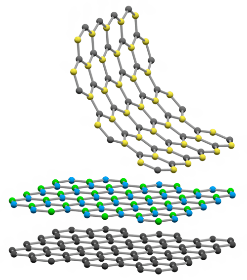
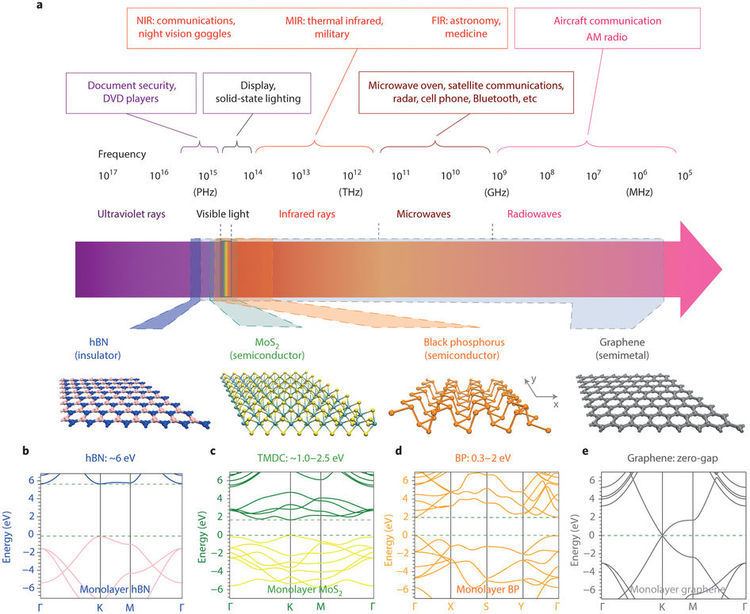
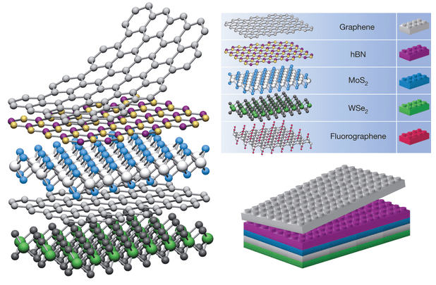
2D materials can generally be categorised as either 2D allotropes of various elements or compounds (usually consisting of two covalently bonding elements). The elemental 2D materials generally carry the -ene suffix in their names while the compounds have -ane or -ide suffixes. Layered combinations of different 2D materials are generally called van der Waals heterostructures. However, the efficient integration of 2D functional layers with three-dimensional (3D) systems remains a significant challenge, limiting device performance and circuit design.
While the first 2D material to be discovered was graphene, in 2004, some 500 2D materials may remain to be found. Research on these other materials has grown more rapidly than that on graphene since 2010.
The global market for 2D materials is expected to reach US$390 million within a decade, mostly for graphene in the semiconductor, electronics, battery energy and composites markets.
The promise of 2d materials
Graphene
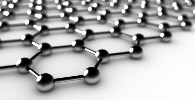
Graphene is a crystalline allotrope of carbon in the form of a nearly transparent (to visible light) one atom thick sheet. It is hundreds of times stronger than most steels by weight. It has the highest known thermal and electrical conductivity, displaying current densities 1,000,000 times that of copper. It was first produced in 2004.
Andre Geim and Konstantin Novoselov won the 2010 Nobel Prize in Physics "for groundbreaking experiments regarding the two-dimensional material graphene". They first produced it by lifting graphene flakes from bulk graphite with adhesive tape and then transferring them onto a silicon wafer.
Graphyne
Graphyne is another 2-dimensional carbon allotrope whose structure is similar to graphene's. It can be seen as a lattice of benzene rings connected by acetylene bonds. Depending on the content of the acetylene groups, graphyne can be considered a mixed hybridization, spn, where 1 < n < 2, and versus graphene's (pure sp2) and diamond (pure sp3).
First-principle calculations using phonon dispersion curves and ab-initio finite temperature, quantum mechanical molecular dynamics simulations showed graphyne and its boron nitride analogues to be stable.
The existence of graphyne was conjectured before 1960. It has not yet been synthesized. However, graphdiyne (graphyne with diacetylene groups) was synthesized on copper substrates. Recently it has been claimed to be a competitor for graphene, due to the potential of direction-dependent Dirac cones.
Borophene
Borophene is a proposed crystalline allotrope of boron. One unit consists of 36 atoms arranged in an 2-dimensional sheet with a hexagonal hole in the middle. Borophene has also been synthesized, but with a different crystal structure.
Germanene
Germanene is a two-dimensional allotrope of germanium, with a buckled honeycomb structure. Experimentally synthesized germanene exhibits a honeycomb structure. This honeycomb structure consists of two hexagonal sub-lattices that are vertically displaced by 0.2 A from each other.
Silicene
Silicene is a two-dimensional allotrope of silicon, with a hexagonal honeycomb structure similar to that of graphene.
Stanene
Stanene is a predicted topological insulator that may display dissipationless currents at its edges near room temperature. It is composed of tin atoms arranged in a single layer, in a manner similar to graphene. Its buckled structure leads to high reactivity against common air pollutions such as NOx and COx and is able to trap and dissociate them at low temperature.
Phosphorene
Phosphorene is a 2-dimensional, crystalline allotrope of phosphorus. Its mono-atomic hexagonal structure makes it conceptually similar to graphene. However, phosphorene has substantially different electronic properties; in particular it possesses a nonzero band gap while displaying high electron mobility. This property potentially makes it a better semiconductor than graphene. The synthesis of phosphorene mainly consists of micromechanical cleavage or liquid phase exfoliation methods. The former has a low yield while the latter produce free standing nanosheets in solvent and not on the solid support. The bottom up approaches like chemical vapor deposition are still blank because of its high reactivity. Therefore, in the current scenario, the most effective method for large area fabrication of thin films of phosphorene consists of wet assembly techniques like Langmuir-Blodgett involving the assembly followed by deposition of nanosheets on solid supports.
Metals
Single atom layers of palladium, and rhodium have also been synthesized.
2D supracrystals
The supracrystals of 2D materials have been proposed and theoretically simulated. These monolayer crystals are built of supra atomic periodic structures where atoms in the nodes of the lattice are replaced by symmetric complexes. For example, in the hexagonal structure of graphene patterns of 4 or 6 carbon atoms would be arranged hexagonally instead of single atoms, as the repeating node in the unit cell.
Graphane
Graphane is a polymer of carbon and hydrogen with the formula unit (CH)
n where n is large. Graphane is a form of fully hydrogenated (on both sides) graphene. Partial hydrogenation is then hydrogenated graphene.
Graphane's carbon bonds are in sp3 configuration, as opposed to graphene's sp2 bond configuration. Thus graphane is a two-dimensional analog of cubic diamond.
The first theoretical description of graphane was reported in 2003 and its preparation was reported in 2009.
Graphane can be formed by electrolytic hydrogenation of graphene, few-layer graphene or high-oriented pyrolytic graphite. In the last case mechanical exfoliation of hydrogenated top layers can be used.
p-doped graphane is postulated to be a high-temperature BCS theory superconductor with a Tc above 90 K.
Properties
Structural
2D boron nitride is an sp2 conjugated compound that forms a honeycomb structure of alternating boron and nitrogen atoms with a lattice spacing of 1.45Å. It adopts the hexagonal (h-BN) allotrope of the three possible crystalline forms of boron nitride because it is the most ubiquitous and stable structure. Boron nitride nanosheets contain two different edges. In the armchair edge structure, the edge consists of either boron or nitrogen atoms. In the zig-zag edge structure, the edge consists of alternating boron and nitrogen atoms. These 2D structures can stack on top of each other and are held by Van der Waal forces to form what is called few-layer boron nitride nanosheets. In these structures, the boron atoms of one sheet are positioned on top or below the nitrogen atoms due to electron deficient nature of boron and electron rich nature of nitrogen, respectively. Due to several similar structural similarities with graphene, boron nitride nanosheets are considered graphene analogs, often called “white graphene".
Boron nanosheets (BNNS) defined as single or few layers of boron nitride whose aspect ratio is small. However, there are a couple variations of 2D boron nitride structure. Boron nitride nanoribbons (BNNR) are boron nitride nanosheets with significant edge effects and have widths that are smaller than 50 nanometers. Boron nitride nanomeshes (BNNM) are boron nitride nanosheets that are placed upon specific metal substrates.
Electrical
Boron nitride nanosheets have a wide bandgap that ranges from 5 to 6 eV and can be changed by the presence of Stone-Wales defects within the structure, by doping or functionalization, or by changing the number of layers. Due to this large bandgap and tunability as well as its surface flatness, boron nitride nanosheets are considered to be an excellent electric insulators and are often used as dielectrics in electrical devices.
Thermal
2D boron nitride structures are excellent thermal conductors, with a thermal conductivity range of 100-270 W/mK. It has been suggested that single layer boron nitride nanosheets have a greater thermal conductivity than other forms of boron nitride nanosheets due to decreased phonon scattering from subsequent layers.
The thermal stability of boron nitride nanosheets is very high due to the high thermal stability properties of hexagonal boron nitride. As single layer and few-layer boron nitride nanosheets begin to oxidize and lose their electrical properties at 800 °C, they are excelle
Synthesis
CVD
Chemical vapor deposition is a popular synthesis method to produce boron nitride because it is a highly controllable process that produces high quality and defect free monolayer and few-layer boron nitride nanosheets. In the majority of CVD methods, boron and nitride precursors react with a metal substrate at high temperature. This allows for nanosheets of a large area as the layers grow uniformly on the substrate. There is a wide range of boron and nitride precursors such as borazine and selection of these precursors depend on factors such as toxicity, stability, reactivity, and the nature of the CVD method. However, despite the high quality of the nanosheets synthesized by chemical vapor deposition, it is not a good method for the large scale production of boron nitride nanosheets for applications.
Mechanical cleavage
While there are several mechanical cleaving methods to produce boron nitride nanosheets, they employ the same principle: using shear forces to break the Van der Waals interactions between the layers of boron nitride. The advantage of mechanical cleavage is that the nanosheets isolated from these techniques have few defects and retain the lateral size of the original substrate.
Inspired by its use in the isolation of graphene, micromechanical cleavage, also known as the Scotch-tape method, has been used to consistently isolate few-layer and monolayer boron nitride nanosheets by subsequent exfoliation of the beginning material with adhesive tape. However, the disadvantage of this technique is that it is not scalable for large scale production.
Ball milling is another technique used to mechanically exfoliate boron nitride sheets from the parent substrate. In this process, shear forces are applied on the face of bulk boron nitride by rolling balls, which break the Van der Waal interactions between each layer. While the ball milling technique may allow for large quantities of boron nitride nanosheets, it does not allow for control the size or the number of layers of the resulting nanosheets. Furthermore, these nanosheets have more defects due to the aggressive nature of this technique. However, improvements such as the addition of a milling agent such as benzyl benzoate or the use of smaller balls has allowed for a greater yield of higher quality nanosheets.
Boron nitride nanosheets have also been isolated by using a vortex fluidic device, which uses centripetal force to shear off layers of boron nitride.
Unzipping of boron nitride nanotubes
Boron nitride nanosheets may also be synthesized by the unzipping of boron nitride nanotubes (BNNT). These nanotubes can be made into sheets by breaking the bonds connecting the N and B atoms by potassium intercalation or by etching by plasma or an inert gas. The unzipping of boron nitride nanotubes by plasma can be used to control the size of the nanosheets, but it produces semiconducting boron nitride nanosheets. The potassium intercalation method produces a low yield of nanosheets as boron nitride is resistive to the effects of intercalants.
Solvent exfoliation and sonication
Solvent exfoliation is often used in tandem with sonication to break the weak Van der Waals interactions present in bulk boron nitride to isolate large quantities of boron nitride nanosheets. Polar solvents such as isopropyl alcohol and DMF have been found to be more effective in exfoliating boron nitride layers than nonpolar solvents because these solvents possess a similar surface energy to the surface energy of boron nitride nanosheets. Combinations of different solvents also exfoliate boron nitride better than when the solvents were used individually. However, many solvents that can be used to exfoliate boron nitride are fairly toxic and expensive. Common solvents such as water and isopropyl alcohol have been determined to be comparable to these toxic polar solvents in exfoliating boron nitride sheets.
Chemical functionalization and sonication
Chemical functionalization of boron nitride involves attaching molecules onto the outer and inner layers of bulk boron nitride. There are three types of functionalization that can be done to boron nitride: covalent functionalization, ionic functionalization, or non covalent functionalization. Layers are then exfoliated by placing the functionalized boron nitride into a solvent and allow the solvation force between the attached groups and the solvent to overcome the Van der Waal forces present in each layer. This method is slightly different than solvent exfoliation as solvent exfoliation relies on the similarities between the surface energies of the solvent and boron nitride layers to overcome the Van der Waals interactions.
Solid State Reactions
The reaction of a mixture of boron and nitrogen precursors at high temperature can produce boron nitride nanosheets. In one method, boric acid and urea were reacted together at 900˚C. The numbers of layers of these nanosheets were controlled by the urea content as well as the temperature
Borocarbonitrides
See also: graphene, boron nitride
Properties
Structural
Borocarbonitrides are two-dimensional compounds that are synthesized such that they contain boron, nitrogen, and carbon atoms in a ratio BxCyNz. Borocarbonitrides are distinct from B,N co-doped graphene in that the former contains seperate boron nitride
and graphene domains as well as rings with B-C, B-N, C-N, and C-C bonds. These compounds generally have a high surface area, but borocarbonitrides synthesized from a high surface area carbon material, urea, and boric acid tend to have the highest surface areas. This high surface area coupled with the presence of Stone-Wales defects in the structure of borocarbonitrides also allows for high absorption of CO2 and CH4, which may make borocarbonitride compounds a useful material in sequestering these gases.
Electrical
The band gap of borocarbonitrides range from 1.0-3.9eV and is dependent on the content of the carbon and boron nitride domains as they have different electrical properties. Borocarbonitrides with a high carbon content have lower bandgaps whereas those with higher content of boron nitride domains have higher band gaps. Borocarbonitrides synthesized in gas or solid reactions also tend to have large bandgaps and are more insulating in character. The wide range of composition of boronitrides allows for the tuning of the bandgap, which when coupled with its high surface area and Stone-Wales defects may make boronitrides a promising material in electrical devices.
Synthesis
Solid state reaction
A high surface area carbon material such as activated charcoal, boric acid, and urea are mixed together and then heated at high temperatures to synthesize borocarbonitride. The composition of the resulting compounds may be changed by varying the concentration of the reagents as well as the temperature.
Gas phase synthesis
In chemical vapor deposition, boron, nitrogen, and carbon precursors react at high heat and are deposited onto a metal substrate. Varying the concentration of precursors and the selection of certain precursors will give different ratios of boron, nitrogen, and carbon in the resulting borocarbonitride compound.
Borocarbonitride composites
Borocarbonitride can also be synthesized by random stacking of boronitride and graphene domains through covalent interactions or through liquid interactions. In the first method, graphene and boron nitride sheets are functionalized and then are reacted to form layers of borocarbonitride. In the second method, boron nitride and graphite powder are dissolved in isopropanol and dimethylformamide, respectively, and then sonicated. This is then exfoliated to isolate borocarbonitride layers.
Germanane
Germanane is a single-layer crystal composed of germanium with one hydrogen bonded in the z-direction for each atom. Germanane’s structure is similar to graphane, Bulk germanium does not adopt this structure. Germanane is produced in a two-step route starting with calcium germanide. From this material, the calcium (Ca) is removed by de-intercalation with HCl to give a layered solid with the empirical formula GeH. The Ca sites in Zintyl-phase CaGe
2 interchange with the hydrogen atoms in the HCl solution, producing GeH and CaCl2.
Molybdenum disulfide
Properties
Structural
Molybdenum disulfide monolayers consist of a unit of one layer of molybdenum atoms covalently bonded to two layers of sulfur atoms While bulk molybdenum sulfide exists as 1T, 2H, or 3R polymorphs, molybdenum disulfide monolayers are found only in the 1T or 2H form. The 2H form adopts a trigonal prismatic geometry while the 1T form adopts an octahedral or trigonal antiprismatic geometry. Molybdenum monolayers can also can be stacked due to Van der Waals interactions between each layer.
Electrical
The electrical properties of molybdenum sulfide in electrical devices depends on factors such as the number of layers, the synthesis method, the nature of the substrate on which the monolayers are placed on, and mechanical strain.
As the number of layers decrease, the band gap begins to increase from 1.2eV in the bulk material up to a value of 1.9eV for a monolayer. Odd number of molybdenum sulfide layers also produce different electrical properties than even numbers of molybednum sulfide layers due to cyclic streching and releasing present in the odd number of layers. Molybdenum sulfide is a p-type material, but it shows ambipolar behavior when molybdenum sulfide monolayers that were 15 nm thick were used in transistors. However, most electrical devices containing molybdenum sulfide monolayers tend to show n-type behavior.
The band gap of molybdenum disulfide monolayers can also be adjusted by applying mechanical strain or an electrical field. Increasing mechanical strain shifts the phonon modes of the molybdenum sulfide layers. This results in a decrease of the band gap and metal-to-insulator transition. Applying an electric field of 2-3Vnm−1 also decreases the indirect bandgap of molybdenum sulfide bilayers to zero.
Solution phase lithium intercalation and exfolation of bulk molybdenum sulfide produces molybdenum sulfide layers with metallic and semiconducting character due to the distribution of 1T and 2H geometries within the material . This is due to the two forms of molybdenum sulfide monolayers having different electrical properties. The 1T polymorph of molybednum sulfide is metallic in character while the 2H form is more semiconducting. However, molybdenum disulfide layers produced by electrochemical lithium intercalation are predominantly 1T and thus metallic in character as there is no conversion to the 2H form from the 1T form.
Thermal
The thermal conductivity of molybdenum disulfide monolayers at room temperature is 34.5W/mK while the thermal conductivity of few-layer molybdenum disulfide is 52W/mK. The thermal conductivity of graphene, on the other hand, is 5300W/mK. Due to the rather low thermal conductivity of molybdenum disulfide nanomaterials, it is not as promising material for high thermal applications as some other 2D materials.
Synthesis
Exfoliation
Exfoliation techniques for the isolating of molybdenum disulfide monolayers include mechanical exfoliation, solvent assisted exfoliation, and chemical exfolation.
Solvent assisted exfoliation is done by sonicating bulk molybdenum disulfide in an organic solvent such as isopropanol and N-methyl-2-pyrrolidone, which disperses the bulk material into nanosheets as the Van der Waals interactions between the layers in the bulk materaial are broken. The amount of nanosheets produced is controlled by the sonication time, the solvent-molybdenum disulfide interactions, and the centrifuge speed. Compared to other exfoliation techniques, solvent assisted exfoliation is the simplest method for large scale production of molybdenum disulfide nanosheets.
The micromechanical exfoliation of molybdenum disulfide was inspired by the same technique used in the isolation of graphene nanosheets. Micromechanical exfoliation alows for low defect molybdenum disulfide nanosheets but is not suitable for large scale production due to low yield.
Chemical exfoliation involves functionalizing molybdenum difsulfide and then sonicating to disperse the nanosheets. The most notable chemical exfoliation technique is lithium intercalation in which lithium is intercalated into bulk molybdenum disulfide and then dispersed into nanosheets by the addition of water.
Chemical vapor deposition (CVD)
Chemical vapor deposition of molybdenum disulfide nanosheets involves reacting molybdenum and sulfur precursors on a substrate at high temperatures. This techinque is often used in the preparing eletrical devices with molybdenum disulfide components because the nanosheets are applied directly on the substrate; unfavorable interactions between the substrate and the nanosheets that would have occured had they been seperately synthesized are decreased. In addition, since the thickness and area of the molybdenum disulfide nanosheets can be controlled by the selection of specific precursors, the electrical properties of the nanosheets can be tuned.
Laser ablation
Pulsed laser deposition involves the thinning of bulk molybdenum disulfide by laser to produce single or multi-layer molybdenum disulfide nanosheets. This allows for synthesis of molybdenum disulfide nanosheets with a defined shape and size. The quality of the nanosheets are determined by the energy of the laser and the irradation angle.
Lasers can also be used to form molybdenum disulfide nanosheets from molybdenum disulfide fullerene-like molecules.
Tungsten diselenide
Tungsten diselenide is an inorganic compound with the formula WSe
2. The compound adopts a hexagonal crystalline structure similar to molybdenum disulfide. Every tungsten atom is covalently bonded to six selenium ligands in a trigonal prismatic coordination sphere, while each selenium is bonded to three tungsten atoms in a pyramidal geometry. The tungsten – selenium bond has a bond distance of 2.526 Å and the distance between selenium atoms is 3.34 Å. Layers stack together via van der Waals interactions. WSe
2 is a stable semiconductor in the group-VI transition metal dichalcogenides.
Hafnium Disulphide
Hafnium Disulphide is a group IVB TMD with formula HfS
2. Like other TMDs, it possess a layered structure with strong covalent bonding between the Hf and S atoms in a layer and weak Van der Wall forces between layers. The compound has CdI
2 type structure and is an indirect band gap semiconducting material. The interlayer spacing between the layers is 0.56 nm, which is small compared to group VIB TMDs like MoS
2, making it difficult to cleave its atomic layers. However, recently its crystals with large interlayer spacing has grown using a chemical vapor transport route. These crystals exfoliate in solvents like N-Cyclohexyl-2-pyrrolidone (CHP) in a time of just some minutes resulting in a high-yield production of its few-layers resulting in increase of its indirect bandgap from 0.9 eV to 1.3 eV. As an application in electronics, its field-effect transistors has been realised using its few layers as a conducting channel material offering a high current modulation ratio larger than 10000 at room temperature. Therefore, group IVB TMDs also holds potential applications in the field of opto-electronics.
MXenes
MXenes are layered transition metal carbides and carbonitrides with general formula of Mn+1XnTx, where M stands for early transition metal, X stands for carbon and/or nitrogen and Tx stands for surface terminations (mostly =O, -OH or -F). MXenes have high electric conductivity (1500 Scm−1) combined with hydrophilic surfaces. This materials show promise in energy storage applications and composites.
Organic
Ni3(HITP)2 is an organic, crystalline, structurally tunable electrical conductor with a high surface area. HITP is an organic chemical (2,3,6,7,10,11-hexaaminotriphenylene). It shares graphene's hexagonal honeycomb structure. Multiple layers naturally form perfectly aligned stacks, with identical 2-nm openings at the centers of the hexagons. Room temperature electrical conductivity is ~40 S cm−1, comparable to that of bulk graphite and among the highest for any conducting Metal-organic frameworks (MOFs). The temperature dependence of its conductivity is linear at temperatures between 100 K and 500 K, suggesting an unusual charge transport mechanism that has not been previously observed in organic semiconductors.
The material was claimed to be the first of a group formed by switching metals and/or organic compounds. The material can be isolated as a powder or a film with conductivity values of 2 and 40 S cm−1, respectively.
Combinations
A 2015 study stacked two different TMD layers onto graphene. This composite displayed negative differential resistance – applying more voltage to the device reduced the current flowing through it.
Characterization of 2D materials
Microscopy techniques such as transmission electron microscopy, scanning probe microscopy, scanning tunneling microscopy, and atomic force microscopy are used to characterize the thickness and size of the 2D materials. Electrical properties and structural properties such as composition and defects are characterized by raman spectroscopy, x-ray diffraction, and x-ray photoelectron spectroscopy.
Applications
As of 2014, none of these materials has been used for large scale commercial applications (with the possible exception of graphene). Despite this, many are under close consideration for a number of industries, in areas including electronics and optoelectronics, sensors, biological engineering, filtration, lightweight/strong composite materials, photovoltaics, medicine, quantum dots, thermal management, ethanol distillation and energy storage, and have enormous potential.
Graphene has been the most studied. In small quantities it is available as a powder and as a dispersion in a polymer matrix, or adhesive, elastomer, oil and aqueous and non-aqueous solutions. The dispersion is claimed to be suitable for advanced composites, paints and coatings, lubricants, oils and functional fluids, capacitors and batteries, thermal management applications, display materials and packaging, inks and 3D-printers’ materials, and barriers and films.