
Produced 2 March 2017 Instruction set AMD64 (x86-64) | Designed by AMD | |
 | ||
Common manufacturer(s) GlobalFoundriesSamsung Cores 4 (essential)4–6 (mainstream)8 (enthusiast)8–32 (server) L1 cache 64 KiB instruction, 32 KiB data per core | ||
Zen is the codename for a computer processor microarchitecture from AMD, and was first used with their Ryzen series of CPUs in February 2017. The first Zen based preview system was demonstrated at E3 2016, and first substantially detailed at an event hosted a block away from the Intel Developer Forum 2016. The first Zen based CPUs codenamed "Summit Ridge" reached the market in early March 2017, with Zen-derived Opteron server processors expected in the second quarter of 2017, and Zen-based APUs expected to follow in the second half of 2017.
Contents
- Design
- History and development
- Advantages over predecessors
- Manufacturing process
- Performance
- Memory
- Power consumption and heat output
- Enhanced security and virtualization support
- Connectivity
- Products
- Server processors
- References
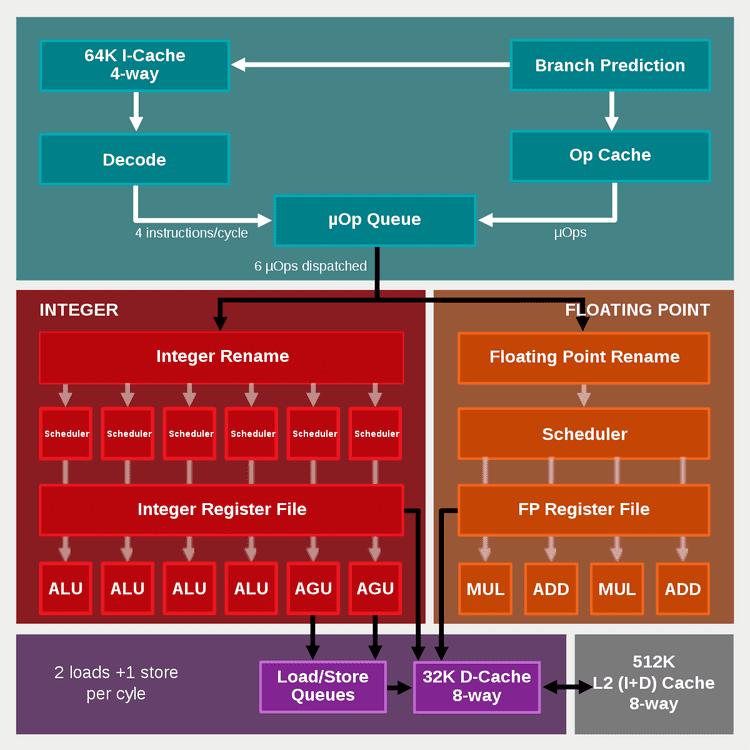
Zen is a clean sheet design that differs from the long-standing Bulldozer architecture. Zen-based processors use a 14 nm FinFET process, are reportedly more energy efficient, and have a significantly higher IPC. SMT has been introduced, allowing each core to run 2 threads. The cache system has also been redesigned, making the L1 cache write-back. Additionally, Zen based processors utilize the AM4 socket, bringing DDR4 support.
Zen is based on a SoC design. The memory, PCIe, SATA, and USB controllers are incorporated into the same chip as the processor cores. This has advantages in bandwidth and power, at the expense of chip complexity and die area. This SoC design will allow the Zen microarchitecture to scale from laptops and small-form factor mini PCs to high-end desktops and servers.
Design
According to AMD, the main focus of Zen is on increasing per-core performance. New or improved features include:
The Zen architecture is built on a 14 nanometer FinFET process subcontracted to GlobalFoundries, giving greater efficiency than the 32 nm and 28 nm processes of previous AMD FX CPUs and AMD APUs, respectively. The "Summit Ridge" Zen family of CPUs use the AM4 socket and feature DDR4 support and a 95 W TDP (thermal design power). While newer roadmaps don't confirm the TDP for desktop products, they suggest a range for low-power mobile products with up to two Zen cores from 5 to 15 W and 15 to 35 W for performance-oriented mobile products with up to four Zen cores.
Each Zen core can decode four instructions per clock cycle and includes a micro-op cache which feeds two schedulers, one each for the integer and floating point segments. Each core has two address generation units, four integer units, and four floating point units. Two of the floating point units are adders, and two are multipliers. There are also improvements in the branch predictor. The L1 cache size is 64 KiB for instructions per core and 32 KiB for data per core. The L2 cache size 512 KiB per core, and the L3 is 1-2 MB per core. L3 caches offer 5x the bandwidth of previous AMD designs.
History and development
AMD began planning the Zen microarchitecture shortly after re-hiring Jim Keller in August 2012. AMD formally revealed Zen in 2015.
The team in charge of Zen was led by Keller (who left in September 2015 after a 3-year tenure) and AMD Senior Fellow Michael Clark.
Zen was originally planned for 2017 following the ARM64-based K12 sister core, but on AMD's 2015 Financial Analyst Day it was revealed that K12 was delayed in favor of the Zen design, to allow it to enter the market within the 2016 timeframe, with the release of first Zen-based processors expected for October 2016.
In November 2015 a source inside AMD reported that Zen microprocessors had been tested and "met all expectations" with "no significant bottlenecks found".
In December 2015, it was rumored that Samsung may be contracted as a fabricator for AMD's 14 nm FinFET processors, including both Zen and AMD's then-upcoming Polaris GPU architecture. This was clarified by AMD's July 2016 announcement that products had been successfully produced on Samsung's 14 nm FinFET process. While AMD stated Samsung would be used "if needed", it was argued this would reduce risk for AMD by decreasing dependence on any one foundry.
Advantages over predecessors
Zen's from-scratch design is notably different from its predecessors, with many different types of changes and enhancements being made across the board in hopes of making Zen more competitive with Intel's architectures, and the software most often built with Intel's processor features in mind.
Manufacturing process
Processors built using Zen utilize 14 nm FinFET silicon. These processors are being produced at GlobalFoundries, though reports state some Zen processors may also be produced at TSMC. Prior to Zen, AMD's smallest process size was 28 nm, as utilized by their Steamroller and Excavator microarchitectures. The immediate competition, Intel's Skylake and Kaby Lake microarchitecture, are also fabricated on 14 nm FinFET; though Intel is planning to begin the release of 10 nm parts later in 2017. In comparison to Intel's 14 nm FinFET, AMD claimed in February 2017 the Zen cores would be 10% smaller. AMD also announced it would be using metal-insulator-metal process to increase the clock speeds and reduce voltages of its Zen products.
For identical designs, these die shrinks would use less current (and power) at the same frequency (or voltage). As CPUs are usually power limited (typically up to ~125 W, or ~45 W for mobile), smaller transistors allow for either lower power at the same frequency, or higher frequency at the same power.
Performance
One of Zen's major goals is to focus on performance per-core, and it is targeting a 40% improvement in instructions per cycle (IPC) over its predecessor. Excavator, in comparison, offered 4–15% improvement over previous architectures. AMD announced the final Zen microarchitecture actually achieved 52% improvement in IPC over Excavator. The inclusion of SMT also allows each core to process up to two threads, increasing processing throughput by better utilizing available resources.
The Zen processors also employ sensors across the chip to dynamically scale frequency and voltage. This allows for the maximum frequency to be dynamically and automatically defined by the processor itself based upon available cooling.
AMD has demonstrated an 8-core/16-thread Zen processor outperforming an equally-clocked Intel Broadwell-E processor in Blender rendering and HandBrake benchmarks.
Zen supports AVX2 but it requires two clock cycles to complete AVX2 instruction compared to Intel's one.
Memory
APUs utilizing the Zen architecture will also support High Bandwidth Memory (HBM). Some older APUs from AMD had to rely on traditional shared DDR3 RAM for video memory.
Zen supports DDR4 memory (up to 8 channels).
Power consumption and heat output
Processors built at the 14 nm node on FinFET silicon should show reduced power consumption and therefore heat over their 28 nm and 32 nm non-FinFET predecessors (for equivalent designs), or be more computationally powerful at equivalent heat output/power consumption.
Zen is also expected to utilize clock gating to further reduce power consumption, reducing the frequency of underutilized portions of the core to save power. This will be through AMD's SenseMI technology, using sensors across the chip to dynamically scale frequency and voltage.
Enhanced security and virtualization support
Zen added the support for AMD's Secure Memory Encryption (SME) and AMD's Secure Encrypted Virtualization (SEV). Secure Memory Encryption is real time memory encryption done per page table entry. This is done utilizing the onboard "Security" Processor (ARM Cortex-A5) at boot time to encrypt each page, allowing any DDR4 memory (including nonvolatile varieties) to be encrypted. AMD SME also makes the contents of the memory more resistant to memory snooping and cold boot attacks.
Connectivity
Incorporating much of a southbridge into the SoC, the Zen CPU include SATA, USB, and PCI Express NVMe links. This can be augmented by available Socket AM4 chipsets which add connectivity options including additional SATA and USB connections, and support for AMD's Crossfire and Nvidia's SLI.
AMD, in announcing its Radeon Instinct line, argued that the upcoming Zen based Naples server CPU would be particularly suited for building deep learning systems. The expected 64 PCIe lanes per Naples CPU allows for 4 Instinct cards to connect at PCIe x16 to a single CPU. This compares favorably to the Intel Xeon line, with only 40 PCIe lanes.
Products
Zen architecture is utilized in latest generation desktop Ryzen CPUs. It is also expected in future Opteron server processors, and APUs.
The first desktop processors without graphics processing unit (codename: "Summit Ridge") were initially expected to start selling at the end of 2016, according to an AMD roadmap; with the first mobile and desktop processors of the AMD Accelerated Processing Unit type (codename: "Raven Ridge") following in late 2017. AMD officially delayed Zen until Q1 of 2017. In August 2016, an early demonstration of the architecture showed an 8 cores/16 threads engineering sample CPU at 3.0 GHz.
In December 2016, AMD officially announced the desktop CPU line under the Ryzen brand for release in Q1 2017. It also confirmed Server processors would be released in Q2 2017, and mobile APUs in H2 2017.
On March 2, 2017, AMD officially launched the first Zen architecture based octacore Ryzen desktop CPUs. The final clock speeds and TDPs for the 3 CPUs released in Q1 of 2017 demonstrated a significantly better performance-per-watt benefits over the last generation K15h (Piledriver) architecture. The octacore Ryzen desktop CPUs demonstrated performance-per-watt comparable to Intel's Broadwell architecture based octacore CPUs.
In March, 2017, AMD also demonstrated an engineering sample of the unreleased server CPU based on Zen architecture. The CPU code-named Naples was configured as a dual socket server platform with each CPU having 32 cores/64 threads.
Server processors
AMD announced in March 2017 it will release a server platform based on Zen, codenamed Naples, in the following quarter. The platform will include 1 and 2 socket systems. The CPUs in multi processor configurations will communicate via AMD's infinity fabric. Each chip support 8 channels of memory and 64 PCIe Gen3 lanes per chip.