.jpg)
Advance Microprocessor
The advanced Intel microprocessors: 80286, 80386.
Intel 80286
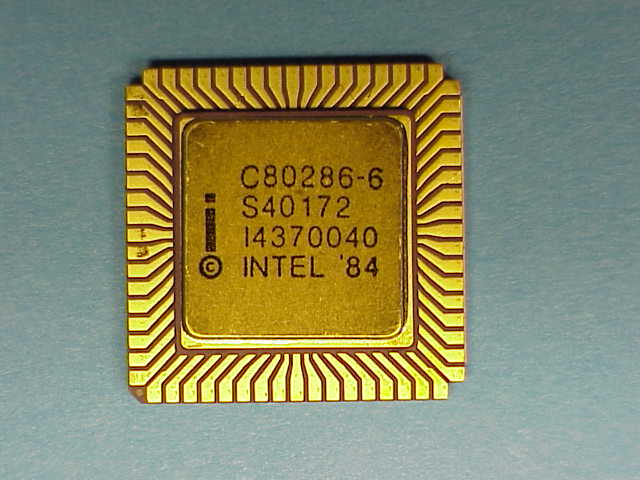
The Intel 80286 ("eighty-two-eighty-six"; also called the iAPX 286, "two-eighty-six"), introduced on 1 February 1982, is a 16-bit x86 microprocessor with 134,000 transistors. Like its contemporary simpler cousin, the 80186, it can correctly execute most software written for the earlier Intel 8086 and 8088. It was employed for the IBM PC/AT, introduced in 1984, and then widely used in most PC/AT compatible computers until the early 1990s. The 80286 was the first x86 microprocessor with memory management and wide protection abilities.
History
After the 6 and 8 MHz initial releases, it was subsequently scaled up to 12.5 MHz. (AMD and Harris later pushed the architecture to speeds as high as 20 MHz and 25 MHz, respectively.) On average, the 80286 had a speed of about 0.21 instructions per clock. The 6 MHz model operated at 0.9 MIPS, the 10 MHz model at 1.5 MIPS, and the 12 MHz model at 2.66 MIPS.
The later E-stepping level of the 80286 was free of the several significant errata that caused problems for programmers and operating system writers in the earlier B-step and C-step CPUs (common in the AT and AT clones).
Architecture

The 80286 was designed for multi-user systems with multitasking applications, including communications (such as automated PBXs) and real-time process control. It had 134,000 transistors and consisted of four independent units: address unit, bus unit, instruction unit and execution unit. These were organized into a pipeline, significantly increasing performance. It was produced in a 68-pin package including PLCC (Plastic Leaded Chip Carrier), LCC (Leadless chip carrier) and PGA (Pin Grid Array) packages.
The performance of the 80286 per clock cycle exceeded that of the Intel 8086 and Intel 8088 by more than two times. This increase of the 80286s performance over its immediate predecessors may be[according to whom?] the largest among the generations of x86 processors. Calculations of the addresses (such as base+index) were less expensive because they were performed by a special unit in the 286. The 8086 had to do effective address computation using its general ALU, which led to a significant clock penalty. Also, the 80286 was more efficient in complex mathematical operations (such as MUL/DIV) than its predecessor.
The intel 80286 had a 24-bit address bus and was able to address up to 16 MB of RAM, compared to 1 MB for its predecessor. However cost and initial rarity of software using the memory above 1 MB meant that 80286 computers were rarely shipped with more than one megabyte of RAM. Additionally, there was a performance penalty involved in accessing extended memory from real mode.
Features
1)Protected mode
An interesting feature of this processor is that it was the first x86 processor with protected mode. Protected mode enabled up to 16 MB of memory to be addressed by the on-chip linear memory management unit (MMU) with 1 GB logical address space. The MMU also provided protection from (crashed or ill-behaved) applications writing outside their allocated memory zones. The MMU and protection mechanisms are enabled only in case of protected mode (except for the segment overrun protection) keeping them disabled in real mode of operation. Several additional instructions were introduced in protected mode of 80286, which are helpful for multitasking operating systems.
Another important feature of 80286 is Prevention of Unauthorised Access. This is achieved by:
1.Forming different segments for data, code, and stack, and preventing their overlapping
2.Assigning Privilege levels to each segment. Segment with lower privilege level cannot access the segment with higher privilege level.
The 80286 provided built in memory protection mechanisms which had been almost exclusive to mainframes and minicomputers (CPUs like the NS320xx and M68000 needed additional components in order to implement MMU functions) and the large performance enhancements represented by the 80286 and many of its successors would pave the way for the x86 and the IBM PC architecture to extend from low performance personal computers all the way to high-end workstations and servers and even drive the market for other architectures.
In 80286 (and in its co-processor Intel 80287), arithmetic operations can be performed on the following different types of numbers:
1.unsigned packed decimal,
2. unsigned binary,
3.unsigned unpacked decimal,
4.signed binary, and
5.floating point numbers.
In theory, real-mode applications could be directly executed in 16-bit protected mode if certain rules were followed; however, as many DOS programs broke those rules, protected mode was not widely used until the appearance of its successor, the 32-bit Intel 80386, which was designed to go back and forth between modes easily. When Intel designed the 286, it was not designed to be able to multitask real-mode applications; real mode was intended to be a simple way for a bootstrap loader to prepare the system and then switch to protected mode.
2)OS support
After its appearance in 1982, the protected mode of the 80286 had not been utilized for many years. For example, in 1986 the only program that made use of it was VDISK, a RAM disk driver included with the PC DOS 3.0 and 3.1. (The DOS could utilize the additional RAM available in the protected mode—extended memory either via BIOS call (INT 15h, AH=87h), or as RAM disk, or as emulation of expanded memory.) The difficulty lay in the incompatibility of old DOS (real mode) programs with protected mode. They simply could not natively run in this new mode without significant modification. In protected mode, memory management and interrupt handling were done differently than in real mode. In addition, DOS programs would not be allowed to access or modify data and code segments that did not belong to them as they could in real mode. The choice that OS system developers faced was either to start from scratch and create an OS that would not run the vast majority of the old programs or to come up with a version of DOS that was slow and ugly but still would run a majority of the old programs.
In January 1985, Digital Research previewed the Concurrent DOS 286 operating system made in cooperation with Intel. The product would function strictly as an 80286 native mode operating system, allowing users to take full advantage of the protected mode to perform multi-user, multitasking operations while running 8086 emulation.This worked on the B-1 prototype step of the chip, but Digital Research discovered problems with the emulation on the production level C-1 step in May, which would not allow Concurrent DOS 286 to run 8086 software in protected mode. The release of Concurrent DOS 286 was delayed until Intel would develop a new version of the chip. In August, after extensive testing E-1 step samples of the 80286, Digital Research acknowledged that Intel corrected all documented 286 errata, but said there were still undocumented chip performance problems with the prerelease version of Concurrent DOS 286 running on the E-1 step. Intel said the approach Digital Research wished to take in emulating 8086 software in protected mode differed from the original specifications. Nevertheless, they implemented minor changes in the microcode that would allow Digital Research to run emulation mode much faster, incorporated into the E-2 step. Named IBM 4680 OS, IBM originally chose DR Concurrent DOS 286 as the basis of their IBM 4680 computer for IBM Plant System products and Point-of-Sale terminals in 1986. The same limitations affected Digital Researchs FlexOS 286 version 1.0, a derivation of Concurrent DOS 286, developed in 1986, introduced in January 1987, and later adopted by IBM for their IBM 4690 OS.
The problems led to Bill Gates famously referring to the 80286 as a "brain dead chip",since it was clear that the new Microsoft Windows environment would not be able to run multiple MS-DOS applications with the 286. It was arguably responsible for the split between Microsoft and IBM, since IBM insisted that OS/2, originally a joint venture between IBM and Microsoft, would run on a 286 (and in text mode).
Other operating systems that used the protected mode of the 286 were Microsoft Xenix (around 1984), Coherent, and Minix. These were less hindered by the limitations of the 80286 protected mode because they did not aim to run MS-DOS programs. In its successor 80386 chip, Intel enhanced the protected mode to address more memory, but also added the separate virtual 8086 mode, which had much better MS-DOS compatibility, in order to satisfy the diverging needs of the market.
Intel 80386
The Intel 80386 ("eighty-three-eighty-six"), also known as the Intel386, i386, or just 386 ("three-eighty-six"), is a 32-bit microprocessor introduced by Intel in 1985. The first versions had 275,000 transistors and were used as the central processing unit (CPU) of many workstations and high-end personal computers of the time. As the original implementation of the 32-bit extension of the 8086 architecture, the 80386 instruction set, programming model, and binary encodings are still the common denominator for all 32-bit x86 processors, this is termed x86, IA-32, or i386-architecture, depending on context.
The 80386 could correctly execute most code intended for earlier 16-bit x86 processors such as the 8088 and 80286 that were ubiquitous in early PCs. Following the same tradition, modern 64-bit x86 processors are able to run most programs written for older chips, all the way back to the original 16-bit 8086 of 1978. Over the years, successively newer implementations of the same architecture have become several hundreds of times faster than the original 80386 (and thousands of times faster than the 8086). A 33 MHz 80386 was reportedly measured to operate at about 11.4 MIPS.
The 80386 was launched in October 1985, but full-function chips were first delivered in the third quarter of 1986. Mainboards for 80386-based computer systems were cumbersome and expensive at first, but manufacturing was rationalized upon the 80386s mainstream adoption. The first personal computer to make use of the 80386 was designed and manufactured by Compaq and marked the first time a fundamental component in the IBM PC compatible de facto-standard was updated by a company other than IBM.
Some mobile phones also used (later fully static CMOS variants of) the 80386 processor, such as BlackBerry 950[8] and Nokia 9000 Communicator.
Architecture

The processor was a significant evolution in the x86 architecture, and extended a long line of processors that stretched back to the Intel 8008. The predecessor of the 80386 was the Intel 80286, a 16-bit processor with a segment-based memory management and protection system. The 80386 added a 32-bit architecture and a paging translation unit, which made it much easier to implement operating systems that used virtual memory. It also offered support for register debugging.
The 80386 featured three operating modes: real mode, protected mode and virtual mode. The protected mode which debuted in the 286 was extended to allow the 386 to avDatatypes of 80386
Datatypes of 80386
The following data types are directly supported and thus implemented by one or more 80386 machine instructions; these data types are described here in brief.
1. Bit (boolean value), bit field (group of up to 32 bits) and bit string (up to 4Gb in length).
2. 8-bit integer (byte), either signed (range -128..127) or unsigned (range 0..255).
3. 16-bit integer, either signed (range -32,768..32,767) or unsigned (range 0..65,535).
4. 32-bit integer, either signed (range -231..231-1) or unsigned (range 0..232-1).
5. 64-bit integer, either signed (range -263..263-1) or unsigned (range 0..264-1).
6. Offset, a 16 or 32-bit displacement referring to a memory location (using any addressing mode).
7. Pointer, a 16-bit selector together with a 16 or 32 bit offset.
8. Character (8-bit character code).
9. String, a sequence of 8, 16 or 32-bit words (up to 4 Gb in length).
10. BCD, decimal digits (0..9) represented by unpacked bytes.
11. Packed BCD, two BCD digits in one byte (range 0..99).
Address up to 4 GB of memory. The all new virtual 8086 mode (or VM86) made it possible to run one or more real mode programs in a protected environment, although some programs were not compatible.
The ability for a 386 to be set up to act like it had a flat memory model in protected mode despite the fact that it uses a segmented memory model in all modes would arguably be the most important feature change for the x86 processor family until AMD released x86-64 in 2003.
Chief architect in the development of the 80386 was John H. Crawford. He was responsible for extending the 80286 architecture and instruction set to 32-bit, and then led the microprogram development for the 80386 chip.The 80486 and P5 Pentium line of processors were descendants of the 80386 design.
Business importance
The first company to design and manufacture a PC based on the Intel 80386 was Compaq. By extending the 16/24-bit IBM PC/AT standard into a natively 32-bit computing environment, Compaq became the first third party to implement a major technical hardware advance on the PC platform. IBM was offered use of the 80386, but had manufacturing rights for the earlier 80286. IBM therefore chose to rely on that processor for a couple of more years. The early success of the Compaq 386 PC played an important role in legitimizing the PC "clone" industry, and in de-emphasizing IBMs role within it.
Prior to the 386, the difficulty of manufacturing microchips and the uncertainty of reliable supply made it desirable that any mass-market semiconductor be multi-sourced, that is, made by two or more manufacturers, the second and subsequent companies manufacturing under license from the originating company. The 386 was for a time only available from Intel, since Andy Grove, Intels CEO at the time, made the decision not to encourage other manufacturers to produce the processor as second sources. This decision was ultimately crucial to Intels success in the market.[citation needed] The 386 was the first significant microprocessor to be single-sourced. Single-sourcing the 386 allowed Intel greater control over its development and substantially greater profits in later years.
AMD introduced its compatible Am386 processor in March 1991 after overcoming legal obstacles, thus ending Intels monopoly on 386-compatible processors. IBM also later manufactured 386 chips under license.
Compatibles
Intel i386 packaged by IBM.
1. The AMD Am386SX and Am386DX were almost exact clones of the 80386SX and 80386DX. Legal disputes caused production delays for several years, but AMDs 40 MHz part eventually became very popular with computer enthusiasts as a low cost and low power alternative to the 25 MHz 486SX. The power draw was further reduced in the "notebook models" (Am386 DXL/SXL/DXLV/SXLV) which could operate with 3.3V and were implemented in fully static CMOS circuitry.
2.Chips and Technologies Super386 38600SX and 38600DX were developed using reverse engineering. They sold poorly, due to some technical errors and incompatibilities, as well as their late appearance on the market. They were therefore short-lived products.
3.Cyrix Cx486SLC/Cx486DLC could be (simplistically) described as a kind of 386/486 hybrid chip that included a small amount of on-chip cache. It was popular among computer enthusiasts but did poorly with OEMs. The Cyrix Cx486SLC and Cyrix Cx486DLC processors were pin-compatible with 80386SX and 80386DX respectively. These processors were also manufactured and sold by Texas Instruments.
4.IBM 386SLC and 486SLC/DLC were variants of Intels design which contained a large amount of on-chip cache (8 kB, and later 16 kB). The agreement with Intel limited their use to IBMs own line of computers and upgrade boards only, so they were not available on the open market.
Early problems
Intel originally intended for the 80386 to debut at 16 MHz. However, due to poor yields, it was instead introduced at 12 MHz.
Early in production, Intel discovered a marginal circuit that could cause a system to return incorrect results from 32-bit multiply operations. Not all of the processors already manufactured were affected, so Intel tested its inventory. Processors that were found to be bug-free were marked with a double-sigma (??), and affected processors were marked "16 BIT S/W ONLY". These latter processors were sold as good parts, since at the time 32 bit capability was not relevant for most users. Such chips are now extremely rare.
The i387 math coprocessor was not ready in time for the introduction of the 80386, and so many of the early 80386 motherboards instead provided a socket and hardware logic to make use of an 80287. In this configuration the FPU would operate asynchronously to the CPU, usually with a clock rate of 10 MHz. The original Compaq Deskpro 386 is an example of such design. However, this was an annoyance to those who depended on floating point performance, as the performance advantages of the 80387 over the 80287 were significant.
Models and variants
Early 5V models
80386DX
Original version, released in October 1985.
1. Capable of working with 16- or 32-bit external busses
2. Cache: depends on mainboard
3. Package: PGA-132 or PQFP-132
4. Process: First types CHMOS III, 1.5 µm, later CHMOS IV, 1 µm
5. Die size: 104 mm² (ca. 10 mm x 10 mm) in CHMOS III and 39 mm² (6 mm x 6.5 mm) in CHMOS IV.
6. Transistor count: 275 000[1]
7. Specified max clock: 12 MHz (early models), later 16, 20, 25 and 33 MHz
RapidCAD
A specially packaged Intel 486DX and a dummy floating point unit (FPU) designed as pin-compatible replacements for an Intel 80386 processor and 80387 FPU.
Versions for embedded systems
This was an embedded version of the 80386SX which did not support real mode and paging in the MMU.
i386EX, i386EXTB and i386EXTC
System and power management and built in peripheral and support functions: Two 82C59A interrupt controllers; Timer, Counter (3 channels); Asynchronous SIO (2 channels); Synchronous SIO (1 channel); Watchdog timer (Hardware/Software); PIO. Usable with 80387SX or i387SL FPUs.
1. Data/address bus: 16 / 26 bits
2. Package: PQFP-132, SQFP-144 and PGA-168
3. Process: CHMOS V, 0.8 µm
4. Specified max clock:
i386EX: 16 MHz @2.7~3.3 volt or 20 MHz @3.0~3.6 volt or 25 MHz @4.5~5.5 volt
i386EXTB: 20 MHz @2.7~3.6 volt or 25 MHz @3.0~3.6 volt
i386EXTC: 25 MHz @4.5~5.5 volt or 33 MHz @4.5~5.5 volt
i386CXSA and i386SXSA (or i386SXTA)
Transparent power management mode, integrated MMU and TTL compatible inputs (only 386SXSA). Usable with i387SX or i387SL FPUs.
Data/address bus: 16 / 26 bits (24 bits for i386SXSA)
Package: PQFP-100
Voltage: 4.5~5.5 volt (25 and 33 MHz); 4.75~5.25 volt (40 MHz)
Process: CHMOS V, 0.8 µm
Specified max clock: 25, 33, 40 MHz
i386CXSB
Transparent power management mode and integrated MMU. Usable with i387SX or i387SL FPUs.
Data/address bus: 16 / 26 bits
Package: PQFP-100
Voltage: 3.0 volt (16 MHz) or 3.3 volt (25 MHz)
Process: CHMOS V, 0.8 µm
Specified max clock: 16, 25 MHz
80386
http://nptel.ac.in/courses/Webcourse-contents/IISc-BANG/Microprocessors%20and%20Microcontrollers/pdf/Teacher_Slides/mod8/M8L1.pdf
what is x86?
The advanced Intel microprocessors: 80286, 80386.
Intel 80286
The Intel 80286 ("eighty-two-eighty-six"; also called the iAPX 286, "two-eighty-six"), introduced on 1 February 1982, is a 16-bit x86 microprocessor with 134,000 transistors. Like its contemporary simpler cousin, the 80186, it can correctly execute most software written for the earlier Intel 8086 and 8088. It was employed for the IBM PC/AT, introduced in 1984, and then widely used in most PC/AT compatible computers until the early 1990s. The 80286 was the first x86 microprocessor with memory management and wide protection abilities.
History
After the 6 and 8 MHz initial releases, it was subsequently scaled up to 12.5 MHz. (AMD and Harris later pushed the architecture to speeds as high as 20 MHz and 25 MHz, respectively.) On average, the 80286 had a speed of about 0.21 instructions per clock. The 6 MHz model operated at 0.9 MIPS, the 10 MHz model at 1.5 MIPS, and the 12 MHz model at 2.66 MIPS.
The later E-stepping level of the 80286 was free of the several significant errata that caused problems for programmers and operating system writers in the earlier B-step and C-step CPUs (common in the AT and AT clones).
Architecture
The 80286 was designed for multi-user systems with multitasking applications, including communications (such as automated PBXs) and real-time process control. It had 134,000 transistors and consisted of four independent units: address unit, bus unit, instruction unit and execution unit. These were organized into a pipeline, significantly increasing performance. It was produced in a 68-pin package including PLCC (Plastic Leaded Chip Carrier), LCC (Leadless chip carrier) and PGA (Pin Grid Array) packages.
The performance of the 80286 per clock cycle exceeded that of the Intel 8086 and Intel 8088 by more than two times. This increase of the 80286s performance over its immediate predecessors may be[according to whom?] the largest among the generations of x86 processors. Calculations of the addresses (such as base+index) were less expensive because they were performed by a special unit in the 286. The 8086 had to do effective address computation using its general ALU, which led to a significant clock penalty. Also, the 80286 was more efficient in complex mathematical operations (such as MUL/DIV) than its predecessor.
The intel 80286 had a 24-bit address bus and was able to address up to 16 MB of RAM, compared to 1 MB for its predecessor. However cost and initial rarity of software using the memory above 1 MB meant that 80286 computers were rarely shipped with more than one megabyte of RAM. Additionally, there was a performance penalty involved in accessing extended memory from real mode.
Features
1)Protected mode
An interesting feature of this processor is that it was the first x86 processor with protected mode. Protected mode enabled up to 16 MB of memory to be addressed by the on-chip linear memory management unit (MMU) with 1 GB logical address space. The MMU also provided protection from (crashed or ill-behaved) applications writing outside their allocated memory zones. The MMU and protection mechanisms are enabled only in case of protected mode (except for the segment overrun protection) keeping them disabled in real mode of operation. Several additional instructions were introduced in protected mode of 80286, which are helpful for multitasking operating systems.
Another important feature of 80286 is Prevention of Unauthorised Access. This is achieved by:
1.Forming different segments for data, code, and stack, and preventing their overlapping
2.Assigning Privilege levels to each segment. Segment with lower privilege level cannot access the segment with higher privilege level.
The 80286 provided built in memory protection mechanisms which had been almost exclusive to mainframes and minicomputers (CPUs like the NS320xx and M68000 needed additional components in order to implement MMU functions) and the large performance enhancements represented by the 80286 and many of its successors would pave the way for the x86 and the IBM PC architecture to extend from low performance personal computers all the way to high-end workstations and servers and even drive the market for other architectures.
In 80286 (and in its co-processor Intel 80287), arithmetic operations can be performed on the following different types of numbers:
1.unsigned packed decimal,
2. unsigned binary,
3.unsigned unpacked decimal,
4.signed binary, and
5.floating point numbers.
In theory, real-mode applications could be directly executed in 16-bit protected mode if certain rules were followed; however, as many DOS programs broke those rules, protected mode was not widely used until the appearance of its successor, the 32-bit Intel 80386, which was designed to go back and forth between modes easily. When Intel designed the 286, it was not designed to be able to multitask real-mode applications; real mode was intended to be a simple way for a bootstrap loader to prepare the system and then switch to protected mode.
2)OS support
After its appearance in 1982, the protected mode of the 80286 had not been utilized for many years. For example, in 1986 the only program that made use of it was VDISK, a RAM disk driver included with the PC DOS 3.0 and 3.1. (The DOS could utilize the additional RAM available in the protected mode—extended memory either via BIOS call (INT 15h, AH=87h), or as RAM disk, or as emulation of expanded memory.) The difficulty lay in the incompatibility of old DOS (real mode) programs with protected mode. They simply could not natively run in this new mode without significant modification. In protected mode, memory management and interrupt handling were done differently than in real mode. In addition, DOS programs would not be allowed to access or modify data and code segments that did not belong to them as they could in real mode. The choice that OS system developers faced was either to start from scratch and create an OS that would not run the vast majority of the old programs or to come up with a version of DOS that was slow and ugly but still would run a majority of the old programs.
In January 1985, Digital Research previewed the Concurrent DOS 286 operating system made in cooperation with Intel. The product would function strictly as an 80286 native mode operating system, allowing users to take full advantage of the protected mode to perform multi-user, multitasking operations while running 8086 emulation.This worked on the B-1 prototype step of the chip, but Digital Research discovered problems with the emulation on the production level C-1 step in May, which would not allow Concurrent DOS 286 to run 8086 software in protected mode. The release of Concurrent DOS 286 was delayed until Intel would develop a new version of the chip. In August, after extensive testing E-1 step samples of the 80286, Digital Research acknowledged that Intel corrected all documented 286 errata, but said there were still undocumented chip performance problems with the prerelease version of Concurrent DOS 286 running on the E-1 step. Intel said the approach Digital Research wished to take in emulating 8086 software in protected mode differed from the original specifications. Nevertheless, they implemented minor changes in the microcode that would allow Digital Research to run emulation mode much faster, incorporated into the E-2 step. Named IBM 4680 OS, IBM originally chose DR Concurrent DOS 286 as the basis of their IBM 4680 computer for IBM Plant System products and Point-of-Sale terminals in 1986. The same limitations affected Digital Researchs FlexOS 286 version 1.0, a derivation of Concurrent DOS 286, developed in 1986, introduced in January 1987, and later adopted by IBM for their IBM 4690 OS.
The problems led to Bill Gates famously referring to the 80286 as a "brain dead chip",since it was clear that the new Microsoft Windows environment would not be able to run multiple MS-DOS applications with the 286. It was arguably responsible for the split between Microsoft and IBM, since IBM insisted that OS/2, originally a joint venture between IBM and Microsoft, would run on a 286 (and in text mode).
Other operating systems that used the protected mode of the 286 were Microsoft Xenix (around 1984), Coherent, and Minix. These were less hindered by the limitations of the 80286 protected mode because they did not aim to run MS-DOS programs. In its successor 80386 chip, Intel enhanced the protected mode to address more memory, but also added the separate virtual 8086 mode, which had much better MS-DOS compatibility, in order to satisfy the diverging needs of the market.
Intel 80386
The Intel 80386 ("eighty-three-eighty-six"), also known as the Intel386, i386, or just 386 ("three-eighty-six"), is a 32-bit microprocessor introduced by Intel in 1985. The first versions had 275,000 transistors and were used as the central processing unit (CPU) of many workstations and high-end personal computers of the time. As the original implementation of the 32-bit extension of the 8086 architecture, the 80386 instruction set, programming model, and binary encodings are still the common denominator for all 32-bit x86 processors, this is termed x86, IA-32, or i386-architecture, depending on context.
The 80386 could correctly execute most code intended for earlier 16-bit x86 processors such as the 8088 and 80286 that were ubiquitous in early PCs. Following the same tradition, modern 64-bit x86 processors are able to run most programs written for older chips, all the way back to the original 16-bit 8086 of 1978. Over the years, successively newer implementations of the same architecture have become several hundreds of times faster than the original 80386 (and thousands of times faster than the 8086). A 33 MHz 80386 was reportedly measured to operate at about 11.4 MIPS.
The 80386 was launched in October 1985, but full-function chips were first delivered in the third quarter of 1986. Mainboards for 80386-based computer systems were cumbersome and expensive at first, but manufacturing was rationalized upon the 80386s mainstream adoption. The first personal computer to make use of the 80386 was designed and manufactured by Compaq and marked the first time a fundamental component in the IBM PC compatible de facto-standard was updated by a company other than IBM.
Some mobile phones also used (later fully static CMOS variants of) the 80386 processor, such as BlackBerry 950[8] and Nokia 9000 Communicator.
Architecture
The processor was a significant evolution in the x86 architecture, and extended a long line of processors that stretched back to the Intel 8008. The predecessor of the 80386 was the Intel 80286, a 16-bit processor with a segment-based memory management and protection system. The 80386 added a 32-bit architecture and a paging translation unit, which made it much easier to implement operating systems that used virtual memory. It also offered support for register debugging.
The 80386 featured three operating modes: real mode, protected mode and virtual mode. The protected mode which debuted in the 286 was extended to allow the 386 to avDatatypes of 80386
Datatypes of 80386
The following data types are directly supported and thus implemented by one or more 80386 machine instructions; these data types are described here in brief.
1. Bit (boolean value), bit field (group of up to 32 bits) and bit string (up to 4Gb in length).
2. 8-bit integer (byte), either signed (range -128..127) or unsigned (range 0..255).
3. 16-bit integer, either signed (range -32,768..32,767) or unsigned (range 0..65,535).
4. 32-bit integer, either signed (range -231..231-1) or unsigned (range 0..232-1).
5. 64-bit integer, either signed (range -263..263-1) or unsigned (range 0..264-1).
6. Offset, a 16 or 32-bit displacement referring to a memory location (using any addressing mode).
7. Pointer, a 16-bit selector together with a 16 or 32 bit offset.
8. Character (8-bit character code).
9. String, a sequence of 8, 16 or 32-bit words (up to 4 Gb in length).
10. BCD, decimal digits (0..9) represented by unpacked bytes.
11. Packed BCD, two BCD digits in one byte (range 0..99).
Address up to 4 GB of memory. The all new virtual 8086 mode (or VM86) made it possible to run one or more real mode programs in a protected environment, although some programs were not compatible.
The ability for a 386 to be set up to act like it had a flat memory model in protected mode despite the fact that it uses a segmented memory model in all modes would arguably be the most important feature change for the x86 processor family until AMD released x86-64 in 2003.
Chief architect in the development of the 80386 was John H. Crawford. He was responsible for extending the 80286 architecture and instruction set to 32-bit, and then led the microprogram development for the 80386 chip.The 80486 and P5 Pentium line of processors were descendants of the 80386 design.
Business importance
The first company to design and manufacture a PC based on the Intel 80386 was Compaq. By extending the 16/24-bit IBM PC/AT standard into a natively 32-bit computing environment, Compaq became the first third party to implement a major technical hardware advance on the PC platform. IBM was offered use of the 80386, but had manufacturing rights for the earlier 80286. IBM therefore chose to rely on that processor for a couple of more years. The early success of the Compaq 386 PC played an important role in legitimizing the PC "clone" industry, and in de-emphasizing IBMs role within it.
Prior to the 386, the difficulty of manufacturing microchips and the uncertainty of reliable supply made it desirable that any mass-market semiconductor be multi-sourced, that is, made by two or more manufacturers, the second and subsequent companies manufacturing under license from the originating company. The 386 was for a time only available from Intel, since Andy Grove, Intels CEO at the time, made the decision not to encourage other manufacturers to produce the processor as second sources. This decision was ultimately crucial to Intels success in the market.[citation needed] The 386 was the first significant microprocessor to be single-sourced. Single-sourcing the 386 allowed Intel greater control over its development and substantially greater profits in later years.
AMD introduced its compatible Am386 processor in March 1991 after overcoming legal obstacles, thus ending Intels monopoly on 386-compatible processors. IBM also later manufactured 386 chips under license.
Compatibles
Intel i386 packaged by IBM.
1. The AMD Am386SX and Am386DX were almost exact clones of the 80386SX and 80386DX. Legal disputes caused production delays for several years, but AMDs 40 MHz part eventually became very popular with computer enthusiasts as a low cost and low power alternative to the 25 MHz 486SX. The power draw was further reduced in the "notebook models" (Am386 DXL/SXL/DXLV/SXLV) which could operate with 3.3V and were implemented in fully static CMOS circuitry.
2.Chips and Technologies Super386 38600SX and 38600DX were developed using reverse engineering. They sold poorly, due to some technical errors and incompatibilities, as well as their late appearance on the market. They were therefore short-lived products.
3.Cyrix Cx486SLC/Cx486DLC could be (simplistically) described as a kind of 386/486 hybrid chip that included a small amount of on-chip cache. It was popular among computer enthusiasts but did poorly with OEMs. The Cyrix Cx486SLC and Cyrix Cx486DLC processors were pin-compatible with 80386SX and 80386DX respectively. These processors were also manufactured and sold by Texas Instruments.
4.IBM 386SLC and 486SLC/DLC were variants of Intels design which contained a large amount of on-chip cache (8 kB, and later 16 kB). The agreement with Intel limited their use to IBMs own line of computers and upgrade boards only, so they were not available on the open market.
Early problems
Intel originally intended for the 80386 to debut at 16 MHz. However, due to poor yields, it was instead introduced at 12 MHz.
Early in production, Intel discovered a marginal circuit that could cause a system to return incorrect results from 32-bit multiply operations. Not all of the processors already manufactured were affected, so Intel tested its inventory. Processors that were found to be bug-free were marked with a double-sigma (??), and affected processors were marked "16 BIT S/W ONLY". These latter processors were sold as good parts, since at the time 32 bit capability was not relevant for most users. Such chips are now extremely rare.
The i387 math coprocessor was not ready in time for the introduction of the 80386, and so many of the early 80386 motherboards instead provided a socket and hardware logic to make use of an 80287. In this configuration the FPU would operate asynchronously to the CPU, usually with a clock rate of 10 MHz. The original Compaq Deskpro 386 is an example of such design. However, this was an annoyance to those who depended on floating point performance, as the performance advantages of the 80387 over the 80287 were significant.
Models and variants
Early 5V models
80386DX
Original version, released in October 1985.
1. Capable of working with 16- or 32-bit external busses
2. Cache: depends on mainboard
3. Package: PGA-132 or PQFP-132
4. Process: First types CHMOS III, 1.5 µm, later CHMOS IV, 1 µm
5. Die size: 104 mm² (ca. 10 mm x 10 mm) in CHMOS III and 39 mm² (6 mm x 6.5 mm) in CHMOS IV.
6. Transistor count: 275 000[1]
7. Specified max clock: 12 MHz (early models), later 16, 20, 25 and 33 MHz
RapidCAD
A specially packaged Intel 486DX and a dummy floating point unit (FPU) designed as pin-compatible replacements for an Intel 80386 processor and 80387 FPU.
Versions for embedded systems
This was an embedded version of the 80386SX which did not support real mode and paging in the MMU.
i386EX, i386EXTB and i386EXTC
System and power management and built in peripheral and support functions: Two 82C59A interrupt controllers; Timer, Counter (3 channels); Asynchronous SIO (2 channels); Synchronous SIO (1 channel); Watchdog timer (Hardware/Software); PIO. Usable with 80387SX or i387SL FPUs.
1. Data/address bus: 16 / 26 bits
2. Package: PQFP-132, SQFP-144 and PGA-168
3. Process: CHMOS V, 0.8 µm
4. Specified max clock:
i386EX: 16 MHz @2.7~3.3 volt or 20 MHz @3.0~3.6 volt or 25 MHz @4.5~5.5 volt
i386EXTB: 20 MHz @2.7~3.6 volt or 25 MHz @3.0~3.6 volt
i386EXTC: 25 MHz @4.5~5.5 volt or 33 MHz @4.5~5.5 volt
i386CXSA and i386SXSA (or i386SXTA)
Transparent power management mode, integrated MMU and TTL compatible inputs (only 386SXSA). Usable with i387SX or i387SL FPUs.
Data/address bus: 16 / 26 bits (24 bits for i386SXSA)
Package: PQFP-100
Voltage: 4.5~5.5 volt (25 and 33 MHz); 4.75~5.25 volt (40 MHz)
Process: CHMOS V, 0.8 µm
Specified max clock: 25, 33, 40 MHz
i386CXSB
Transparent power management mode and integrated MMU. Usable with i387SX or i387SL FPUs.
Data/address bus: 16 / 26 bits
Package: PQFP-100
Voltage: 3.0 volt (16 MHz) or 3.3 volt (25 MHz)
Process: CHMOS V, 0.8 µm
Specified max clock: 16, 25 MHz
80386
http://nptel.ac.in/courses/Webcourse-contents/IISc-BANG/Microprocessors%20and%20Microcontrollers/pdf/Teacher_Slides/mod8/M8L1.pdf
what is x86?