
 | ||
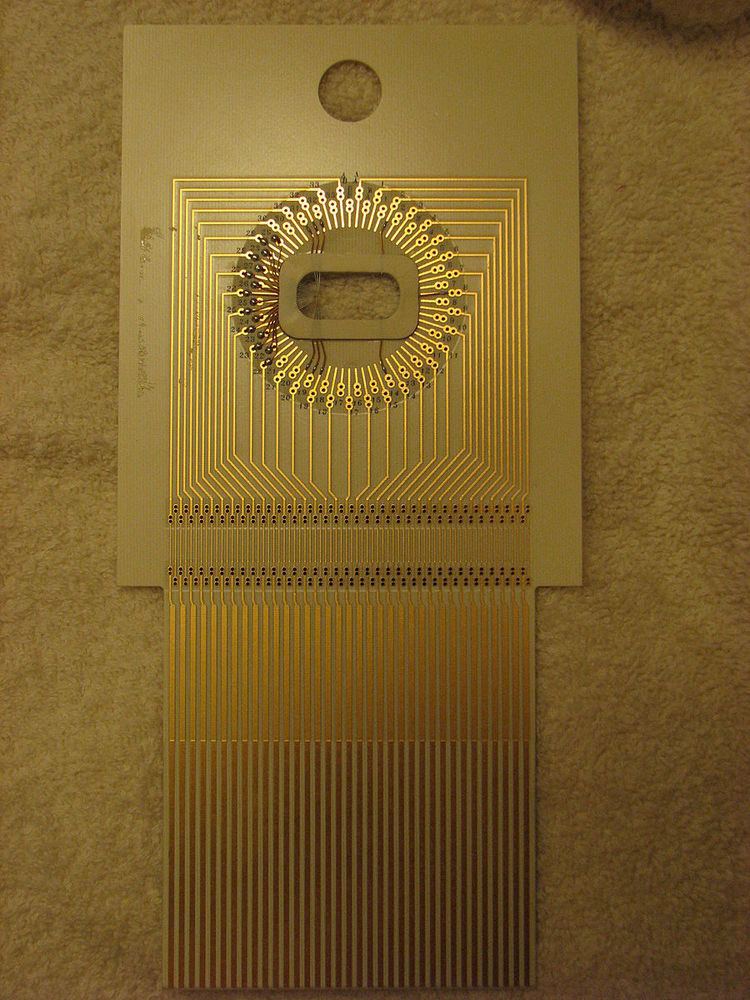
A probe card is an interface between an electronic test system and a semiconductor wafer. Typically the probe card is mechanically docked to a prober and electrically connected to a tester. Its purpose is to provide an electrical path between the test system and the circuits on the wafer, thereby permitting the testing and validation of the circuits at the wafer level, usually before they are diced and packaged. It consists, normally, of a printed circuit board (PCB) and some form of contact elements, usually metallic, but possibly of other materials as well.
A semiconductor manufacturer will typically require a new probe card for each new device wafer and for device shrinks (when the manufacture reduces the size of the device but keep the functions the same) because the probe card is effectively a custom connector that takes the universal pattern of a given tester and translates the signals to connect to electrical pads on the wafer. For testing of DRAM and FLASH memory devices these pads are typically made of aluminum and are 40-90 um per side. Other devices may have flat pads, or raised bumps or pillars made of copper, copper alloys or many types of solders such as lead-tin, tin-silver and others.
The probe card must make good electrical contact to these pads or bumps during the testing of the device. When the testing of the device is complete, the prober will index the wafer to the next device to be tested.
Probe cards are broadly classified into needle type, vertical type, and MEMS(Micro Electro-Mechanical System) type depending on shape and forms of contact elements. MEMS type is the most advanced technology currently available. The most advanced type of probe card currently can test an entire 12" wafer with one touchdown.
Normally a probe card is inserted into an equipment called a wafer prober, inside which position of the wafer to be tested will be manipulated so that there should be a precise contact between the probe card and wafer. Once the probe card and the wafer is loaded, a camera in the prober will optically locate several tips on the probe card and several marks or pads on the wafer, and using this information it can align the pads on the device under test (DUT) to the probe card contacts.
Probe card efficiency is affected by many factors. Perhaps the most important factor impacting probe card efficiency is the number of DUTs that can be tested in parallel. Many wafers today are still tested one device at a time. If one wafer had 1000 of these devices and the time required to test one device was 10 seconds and the time for the prober to move from one device to another device was 1 second, then to test an entire wafer would take 1000 x 11 seconds = 11,000 seconds or roughly 3 hours. If however, the probe card and the tester could test 16 devices in parallel (with 16 times the electrical connections) than the test time would be reduced by almost exactly 16 times. Note that because now the probe card has 16 devices, as the prober touches down on the round wafer, it may not always contact an active device and will therefore be a little less than 16 times as fast to test one wafer.
Another major factor is debris that accumulates on the tips of the probe needles. Normally these are made of tungsten or a tungsten/rhenium alloy although modern probe cards often have contact tips manufactured by MEMS technologies.
Irrespective of the probe tip material, contamination builds up on the tips as a result of successive touch down events (where the probe tips make physical contact with the bond pads of the die). Accumulation of debris has an adverse effect on the critical measurement of contact resistance. To return a used probe card to a contact resistance that is acceptable the probe tips need to be thoroughly cleaned. Cleaning can be done offline using an NWR style laser to reclaim the tips by selectively removing the contamination. Online cleaning can be used during testing to optimize the testing results within the wafer or within wafer lots.