
 | ||
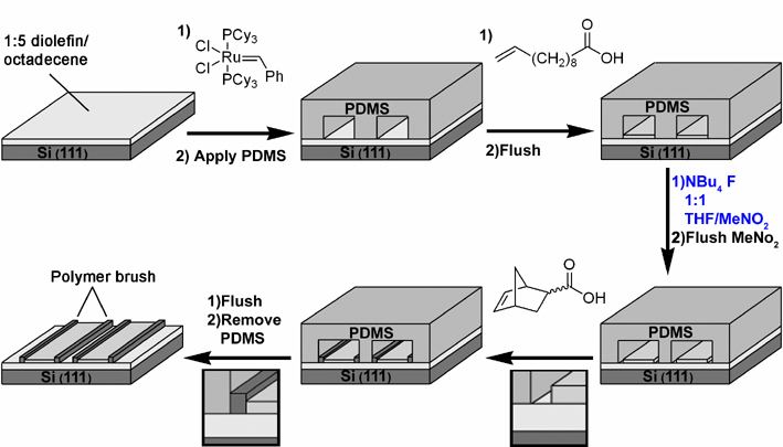
Patterning by Etching at the nanoscale (PENs) is a soft lithographic technique in which the bonds in the polydimethylsiloxane (PDMS) matrix are broken to controlably etch PDMS (i.e. dissolve) at a slow rate along the outside of a PDMS channel formed with a patterned PDMS stamp applied to a surface. The channel in the stamp can be enlarged in the order of tens of nanometers to several micrometres. Exposing a fresh area of a surface that can be reacted with.
Summary
PDMS contains polymer chains of silicon-oxygen bonds, these bonds can be broken by fluoride containing species, in the same way that silicon wafers are prepared by etching with hydrofluoric acid, ammonium fluoride and related compounds. By placing a PDMS stamp that contains a channel that can be externally filled on to a surface, that surface can be functionalised in the area of the channel. By then running an etching solution through the channel, part of the PDMS will be removed. Exposing a fresh area of the surface. This can then be functionaliesd by appropriate chemistry. The width of feature produced is controlled by etchant and time.
To apply this technique for the production of small patterned features it is necessary that the surface can be reacted to passivate it in the area exposed by the channel, followed by etching and then reacted in away that will only occur in the newly exposed area.