
 | ||
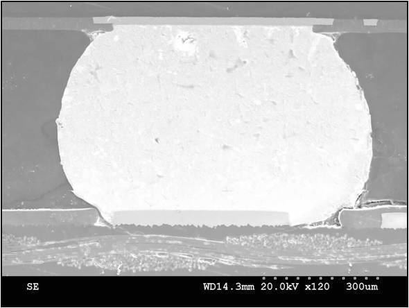
Pad cratering is a mechanically induced fracture in the resin between copper foil and outermost layer of fiberglass of a printed circuit board (PCB). It may be within the resin or at the resin to fiberglass interface.
The pad remains connected to the component (usually a Ball Grid Array, BGA) and leaves a "crater" on the surface of the printed circuit board.
IPC T-50, Revision H, Terms and Definitions for Interconnecting and Packaging Electronic Circuits, 96.2176 - Pad Cratering. A separation of the pad from the printed board resin/weave composite or within the composite immediately adjacent to the pad as a result of mechanical and/or thermal stress.
References
Pad cratering Wikipedia(Text) CC BY-SA