
 | ||
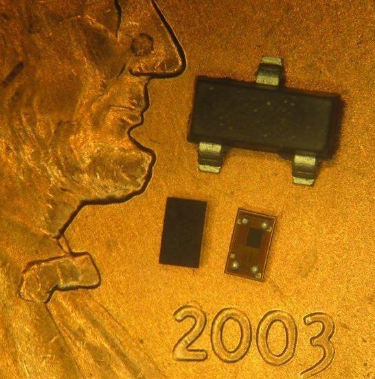
A chip scale package or chip-scale package (CSP) is a type of integrated circuit package.
Originally, CSP was the acronym for chip-size packaging. Since only a few packages are chip size, the meaning of the acronym was adapted to chip-scale packaging. According to IPC’s standard J-STD-012, Implementation of Flip Chip and Chip Scale Technology, in order to qualify as chip scale, the package must have an area no greater than 1.2 times that of the die and it must be a single-die, direct surface mountable package. Another criterion that is often applied to qualify these packages as CSPs is their ball pitch should be no more than 1 mm.
The concept was first proposed by Junichi Kasai of Fujitsu and Gen Murakami of Hitachi Cable. The first concept demonstration however came from Mitsubishi Electric.
The die may be mounted on an interposer upon which pads or balls are formed, like with flip chip ball grid array (BGA) packaging, or the pads may be etched or printed directly onto the silicon wafer, resulting in a package very close to the size of the silicon die: such a package is called a wafer-level package (WLP) or a wafer-level chip-scale package (WL-CSP). WL-CSP had been in development since 1990s, and several companies begun volume production in early 2000, such as Advanced Semiconductor Engineering (ASE).
Types of chip scale packages
Chip scale packages can be classified into the following groups:
- Customized leadframe-based CSP (LFCSP)
- Flexible substrate-based CSP
- Flip-chip CSP (FCCSP)
- Rigid substrate-based CSP
- Wafer-level redistribution CSP (WL-CSP)