
Common manufacturer(s) AMD Instruction set x86-64 Predecessor Family 10h (K10) | Min. feature size 32 nm Socket(s) Socket AM3+ | |
 | ||
Produced From late 2011 to present | ||
The AMD Bulldozer Family 15h is a microprocessor microarchitecture for the FX and Opteron line of processors, developed by AMD for the desktop and server markets. Bulldozer is the codename for this family of microarchitectures. It was released on October 12, 2011 as the successor to the K10 microarchitecture.
Contents
- Overview
- Bulldozer core
- Instruction set extensions
- Process technology and clock frequency
- Cache and memory interface
- IO and socket interface
- Processors
- Desktop
- Server
- False advertising lawsuit
- Performance on Linux
- Performance on Windows
- Overclocking
- Revisions
- References
Bulldozer is designed from scratch, not a development of earlier processors. The core is specifically aimed at computing products with TDPs of 10 to 125 watts. AMD claims dramatic performance-per-watt efficiency improvements in high-performance computing (HPC) applications with Bulldozer cores.
The Bulldozer cores support most of the instruction sets implemented by Intel processors available at its introduction (including SSE4.1, SSE4.2, AES, CLMUL, and AVX) as well as new instruction sets proposed by AMD; ABM, XOP, FMA4 and F16C.
Overview
According to AMD, Bulldozer-based CPUs are based on GlobalFoundries' 32 nm Silicon on insulator (SOI) process technology and reuses the approach of DEC for multitasking computer performance with the arguments that it, according to press notes, "balances dedicated and shared computer resources to provide a highly compact, high units count design that is easily replicated on a chip for performance scaling." In other words, by eliminating some of the "redundant" elements that naturally creep into multicore designs, AMD has hoped to take better advantage of its hardware capabilities, while using less power.
Bulldozer-based implementations built on 32nm SOI with HKMG arrived in October 2011 for both servers and desktops. The server segment included the dual chip (16-core) Opteron processor codenamed Interlagos (for Socket G34) and single chip (4, 6 or 8 cores) Valencia (for Socket C32), while the Zambezi (4, 6 and 8 cores) targeted desktops on Socket AM3+.
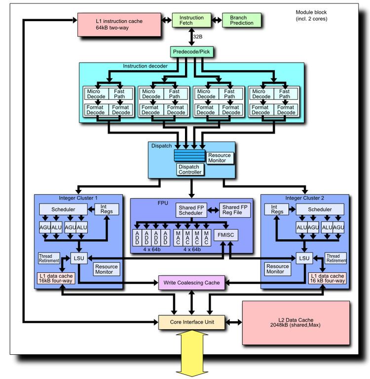
Bulldozer is the first major redesign of AMD’s processor architecture since 2003, when the firm launched its K8 processors, and also features two 128-bit FMA-capable FPUs which can be combined into one 256-bit FPU. This design is accompanied by two integer clusters, each with 4 pipelines (the fetch/decode stage is shared). Bulldozer also introduced shared L2 cache in the new architecture. AMD calls this design a "Module". A 16-core processor design would feature eight of these "modules", but the operating system will recognize each "module" as two logical cores.
The modular architecture consists of multithreaded shared L2 cache and FlexFPU, which uses simultaneous multithreading. Each physical integer core, two per module, is single threaded, in contrast with Intel's Hyperthreading, where two virtual simultaneous threads share the resources of a single physical core.
Bulldozer core
Bulldozer introduced a "Clustered MultiThreading"(CMT) where some parts of the processor are shared between two threads and some parts are unique for each thread.
In terms of hardware complexity and functionality, the Bulldozer CMT module is equal to a dual-core processor in its integer power, and to either a single-core processor or a dual core in its floating-point power, depending on whether the code is saturated in floating point instructions in both threads running on the same CMT module, and whether the FPU is performing 128-bit or 256-bit floating point operations. The reason for this is that for each two integer cores, there is a floating-point unit consisting of a pair of 128-bit FMAC execution units.
CMT is a simpler alternate design philosophy to SMT; both designs try to utilize execution units efficiently; in either method, when two threads compete for some execution pipelines, there is a loss in performance in one or more of the threads. Due to dedicated integer cores, the Bulldozer family modules performed roughly like a dual core dual thread processor during sections of code that were either wholly integer or a mix of integer and floating point; yet, due to the SMT use of the shared floating point pipelines, the module would perform similarly to a single core dual thread SMT processor (SMT2) for a pair of threads saturated with floating point instructions. (Both of these last two comparisons make the assumption that the comparison processor possesses and equally wide and capable execution core, integer-wise and floating-point wise, respectively.)
Both CMT and SMT are at peak effectiveness while running integer and floating point code on a pair of threads. CMT stays at peak effectiveness while working on a pair threads consisting both of integer code, while under SMT, one or both threads will underperform due to competition for integer execution units. The disadvantage for CMT is a greater number of idle integer execution units in a single threaded case. In the single threaded case, CMT is limited to use at most half of the integer execution units in its module, while SMT imposes no such limit. A large SMT core with integer circuitry as wide and fast as two CMT cores could in theory have momentarily up to twice an integer performance in a single thread case. (More realistically for general code as a whole, Pollack's Rule estimates a speedup factor of
CMT processors and a typical SMT processor are similar in their efficient shared use of the L2 cache between a pair of threads.
- each one consists of two ALU and two AGU which are capable of a total of four independent arithmetic and memory operations per clock and per cluster
- duplicating integer schedulers and execution pipelines offers dedicated hardware to each of two threads which double performance for multi-threaded integer loads
- the second integer cluster increases the Bulldozer core die by around 12%, which at chip level adds about 5% of total die space
The longer pipeline allowed the Bulldozer family of processors to achieve a much higher clock frequency compared to its K10 predecessors. While this increased frequencies and throughput, the longer pipeline also increased latencies and increased branch misprediction penalties.
The issue widths (and peak instruction executions per cycle) of a Jaguar, K10, and Bulldozer core are 2, 3, and 4 respectively. This made Bulldozer a more superscalar design compared to Jaguar/Bobcat. However, due to K10's somewhat wider core (in addition to the lack of refinements and optimizations in a first generation design) the Bulldozer architecture typically performed with somewhat lower IPC compared to its K10 predecessors. It was not until the refinements made in Piledriver and Steamroller, that the IPC of the Bulldozer family distinctly began to exceed that of K10 processors such as Phenom II.
Instruction set extensions
Process technology and clock frequency
Cache and memory interface
I/O and socket interface
Processors
The first revenue shipments of Bulldozer-based Opteron processors was announced on September 7, 2011. The FX-4100, FX-6100, FX-8120 and FX-8150 were released in October 2011; with remaining FX series AMD processors released at the end of the first quarter of 2012.
Desktop
Major Sources: CPU-World and Xbit-Labs
Server
There are two series of Bulldozer-based processors for servers: Opteron 4200 series (Socket C32, code named Valencia, with up to four modules) and Opteron 6200 series (Socket G34, code named Interlagos, with up to 8 modules).
False advertising lawsuit
In November 2015, AMD was sued under the California Consumers Legal Remedies Act and Unfair Competition Law for allegedly misrepresenting the specifications of Bulldozer chips. The class-action lawsuit, filed on 26 October in the US District Court for the Northern District of California, claims that the Bulldozer CPU does not have eight cores as advertised, but were effectively quad-core chips due to their module count.
Performance on Linux
On 24 October 2011, the first generation tests done by Phoronix confirmed that the performance of Bulldozer CPU is somewhat less than expected. In many tests the CPU has performed on same level as older generation Phenom 1060T.
The performance later substantially increased, as various compiler optimizations and CPU driver fixes were released.
Performance on Windows
The first Bulldozer CPUs were met with a mixed response. It was discovered that the FX-8150 performed poorly in benchmarks that were not highly threaded, falling behind the second-generation Intel Core i* series processors and being matched or even outperformed by AMD's own Phenom II X6 at lower clock speeds. In highly threaded benchmarks, the FX-8150 performed on par with the Phenom II X6, and the Intel Core i7 2600K, depending on the benchmark. Given the overall more consistent performance of the Intel Core i5 2500K at a lower price, these results left many reviewers underwhelmed. The processor was found to be extremely power-hungry under load, especially when overclocked, compared to Intel's Sandy Bridge.
On 13 October 2011, AMD stated on its blog that "there are some in our community who feel the product performance did not meet their expectations", but showed benchmarks on actual applications where it outperformed the Sandy Bridge i7 2600k and AMD X6 1100T.
In January 2012, Microsoft released two hotfixes for Windows 7 and Server 2008 R2 that marginally improve the performance of Bulldozer CPUs by addressing the thread scheduling concerns raised after the release of Bulldozer.
On 6 March 2012, AMD posted a knowledge base article stating that there was a compatibility problem with FX processors, and certain games on the widely used digital game distribution platform, Steam. AMD stated that they had provided a BIOS update to several motherboard manufacturers (namely: Asus, Gigabyte Technology, MSI, and ASRock) that would fix the problem.
In September 2014, AMD CEO Rory Read conceded the Bulldozer design had not been a "game-changing part", and that AMD had to live with the design for four years.
In July 29, 2015 Microsoft released the Direct X 12 API (DX12) for its Windows 10 operating system. This API allows programmers to achieve greater parallelism, notably in graphics intensive game titles. DX12 titles make better use of the higher core counts and high thread count processor such as the Bulldozer family's FX-6300 and FX-8100 series chips, extending the usability of these systems under Windows 10.
Overclocking
On 31 August 2011, AMD and a group of well-known overclockers including Brian McLachlan, Sami Mäkinen, Aaron Schradin, and Simon Solotko managed to set a new world record for CPU frequency using the unreleased and overclocked FX-8150 Bulldozer processor. Before that day, the record sat at 8.309 GHz, but the Bulldozer combined with liquid helium cooling reached a new high of 8.429 GHz. The record has since been overtaken at 8.58 GHz by Andre Yang using liquid nitrogen. On August 22, 2014 and using an FX-8370 (Piledriver), The Stilt from Team Finland achieved a maximum CPU frequency of 8.722 GHz.
Revisions
Piledriver is the AMD codename for its improved second-generation microarchitecture based on Bulldozer. AMD Piledriver cores are found in Socket FM2 Trinity and Richland based series of APUs and CPUs and the Socket AM3+ Vishera based FX-series of CPUs. Piledriver was the last generation in the Bulldozer family to be available for socket AM3+ and to be available with an L3 cache. The Piledriver processors available for FM2 (and its mobile variant) sockets did not come with a L3 cache, as the L2 cache is the last-level cache for all FM2/FM2+ processors.
Steamroller is the AMD codename for its third-generation microarchitecture based on an improved version of Piledriver. Steamroller cores are found in the Socket FM2+ Kaveri based series of APUs and CPUs.
On 12 October 2011, AMD revealed Excavator to be the codename for the fourth-generation Bulldozer core. Excavator will initially be implemented in the 4th Generation A-series Fusion APU line in 2015. Reports indicated that this APU was codenamed Carrizo. A new low latency L2 cache design derived from the Zen design project was used in the Excavator core, and typically, yet not always, improved performance, due the trade-off between low latency with smaller size (inclusive 1MB per module versus non-inclusive 2MB per module).
The last generation of mainstream processors in the Bulldozer family are codenamed Bristol Ridge (BR). These APUs revised the Carrizo design for socket compatibility with AM4 (or FP4), and included numerous improvements, notably in the areas of power efficiency and graphics. The use of DDR4 in BR allows for a more capable iGPU due to higher memory bandwidth over DDR3 systems. Socket compatibility with Zen AM4 CPUs and APUs allows for a smoother transition from the Bulldozer family of processors to the Zen family of processors. This move to a new generation of large-core and highly superscalar architecture was required by the competitive pressure from later generations of the large-core Intel Core series processors. The new Zen architecture's nearly twice as wide core (4 ALU, 2 AGU, and dedicated floating point circuitry consisting of two dual-issue 128-bit FMAC units) allows AMD to address the Bulldozer family's most urgent limitation of its relatively modest single-threaded IPC (and its competitive disadvantage in lightly threaded yet demanding workloads). In contrast to Bulldozer, the Zen design is wide-core and highly superscalar (12-wide: 6-wide integer, 4-wide FPUs, 2-wide AES), is SMT capable, and has a 4-wide pair of dual-issue FPUs per physical core; furthermore, it was designed to target a much newer 14 nm FinFET fabrication process.