CPUID code 0306D4h L2 cache 256 KB per core | L1 cache 64 KB per core L3 cache 2–6 MB (shared) | |
 | ||
Product code 80658 (mainstream desktop/mobile, Xeon E3)80660 (Xeon E5)80669 (Xeon E7)80671 (enthusiast desktop)80674 (Xeon D) Cores 2–4 (mainstream)6–10 (enthusiast)4–22 (Xeon) | ||
Broadwell microarchitecture
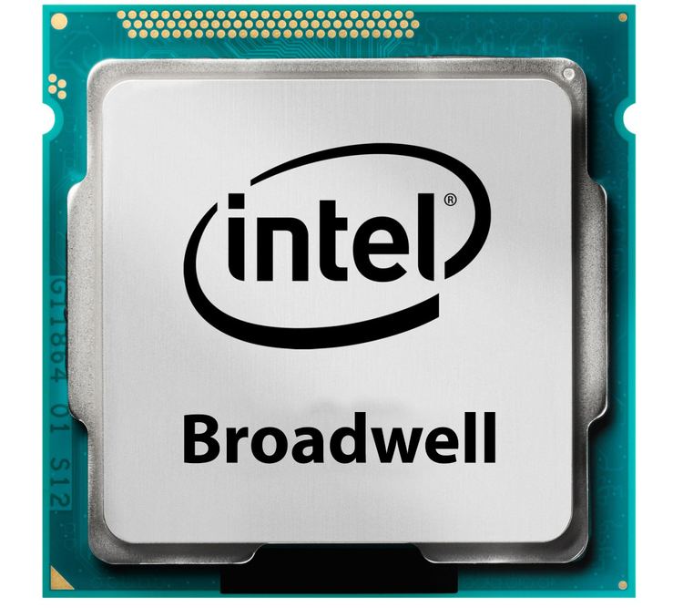
Broadwell is Intel's codename for the 14 nanometer die shrink of its Haswell microarchitecture. It is a "tick" in Intel's tick-tock principle as the next step in semiconductor fabrication. Like some of the previous tick-tock iterations, Broadwell will not completely replace the full range of CPUs from the previous microarchitecture (Haswell), as there will be no low-end desktop CPUs based on Broadwell.
Contents
- Broadwell microarchitecture
- Design and variants
- Instruction set extensions
- New features
- Mobile processors
- Roadmap and history
- Releases
- References
Some of the processors based on the Broadwell microarchitecture are marketed as "5th-generation Core" i3, i5 and i7 processors. This moniker is however not used for marketing of the Broadwell-based Celeron, Pentium or Xeon chips. This microarchitecture also introduced the Core M processor branding.
Broadwell's H and C variants will be used in conjunction with Intel 9 Series chipsets (Z97, H97 and HM97), in addition to retaining backward compatibility with some of the Intel 8 Series chipsets.
Broadwell microarchitecture
Design and variants
Broadwell has been launched in three major variants:
Instruction set extensions
Broadwell introduces some instruction set architecture extensions:
ADOX and ADCX for improving performance of arbitrary-precision integer operationsRDSEED for generating 16-, 32- or 64-bit random numbers from a thermal noise entropy stream, according to NIST SP 800-90B and 800-90CPREFETCHW instructionNew features
Broadwell's Intel Quick Sync Video hardware video decoder adds VP8 hardware decoding and encoding support. It adds VP9 and HEVC 10-bit decoding support through the integrated GPU. Also, it will have two independent bit stream decoder (BSD) rings to process video commands on GT3 GPUs; this will allow one BSD ring to process decoding and the other BSD ring to process encoding at the same time.
Broadwell's integrated GPU supports on Windows Direct3D 11.2, OpenGL 4.4 (OpenGL 4.5 on Linux) and OpenCL 2.0. However, it is marketed as Direct3D-12-ready. Broadwell-E introduced Intel Turbo Boost Max Technology 3.0.
Mobile processors
- When a cooler or quieter mode of operation is desired, this mode specifies a lower TDP and lower guaranteed frequency versus the nominal mode.
- This is the processor's rated frequency and TDP.
- When extra cooling is available, this mode specifies a higher TDP and higher guaranteed frequency versus the nominal mode.
Roadmap and history
On September 10, 2013, Intel showcased the Broadwell 14 nm processor in a demonstration at IDF. Intel CEO Brian Krzanich claimed that the chip would allow systems to provide a 30 percent improvement in power use over the Haswell chips released in mid-2013. Krzanich also claimed that the chips would ship by the end of 2013; however, the shipment was delayed due to low yields from Intel's 14 nm process.
On October 21, 2013, a leaked Intel roadmap indicated a late 2014 or early 2015 release of the K-series Broadwell on the LGA 1150 platform, in parallel with the previously announced Haswell refresh. This will coincide with the release of Intel's 9-series chipset, which may be required for Broadwell processors due to a change in power specifications for its LGA 1150 socket.
On May 18, 2014, Reuters quoted Intel's CEO promising that Broadwell-based PCs will be on shelves for the holiday season, but probably not for the back-to-school shopping.
Mobile CPUs are expected in Q4 2014 and high-performance quad-core CPUs in 2015. The mobile CPUs will benefit from the reduced energy consumption of the die shrink.
On June 18, 2014, Intel told CNET that while some specialized Broadwell-based products would be out in Q4 2014, "broader availability" (including mobile CPUs) would only happen in 2015.
As of July 2014, Broadwell CPUs are available to Intel's hardware partners in sample quantities. Intel is expected to release 17 Broadwell U series family microprocessors at CES 2015. Also, according to a leak posted on vr-zone, Broadwell-E chips will be available in 2016.
On August 11, 2014, Intel unveiled formally its 14 nm manufacturing process, which is used for Broadwell, and indicated that mobile variants of the process will be known as Core M products. Additionally, Core M products were announced to be shipping during the end of 2014, with desktop variants shipping shortly after.
With Broadwell, Intel focused mainly on laptops, miniature desktops, and all-in-one systems. This left traditional desktop users with no new socketed CPU options beyond fourth-generation Haswell, which first arrived in 2013. Even though the company finally introduced two Broadwell desktop chips in the summer of 2015, it launched its high-end sixth-generation Skylake CPUs very shortly thereafter. In September 2015, Kirk Skaugen, senior vice president and general manager of Intel's Client Computing Group, admitted that skipping desktops with Broadwell was a poor decision. Between the end-of-life for Windows XP in 2014 and the lack of new desktop chips, Intel has not given desktop PC users any good reasons to upgrade in 2015.
Releases
On September 5, 2014, Intel launched the first three Broadwell-based processors that belong to the low-TDP Core M family, Core M 5Y10, Core M 5Y10a and Core M 5Y70.
On October 9, 2014, the first laptop with Broadwell Intel Core M 5Y70 CPU, Lenovo Yoga 3 Pro, was launched.
On October 31, 2014, four more Broadwell based CPUs were launched belonging to Core M Family, increasing the number of launched Broadwell CPUs to seven.
On January 5, 2015, 17 additional Broadwell laptop CPUs were launched for the Celeron, Pentium and Core i3, i5 and i7 series.
On March 31, 2016, Intel officially launched 14 nm Broadwell-EP Xeon E5 V4 CPUs.
On May 30, 2016, Intel officially launched 14 nm Broadwell-E Core i7 69xx/68xx processor family.
