
 | ||
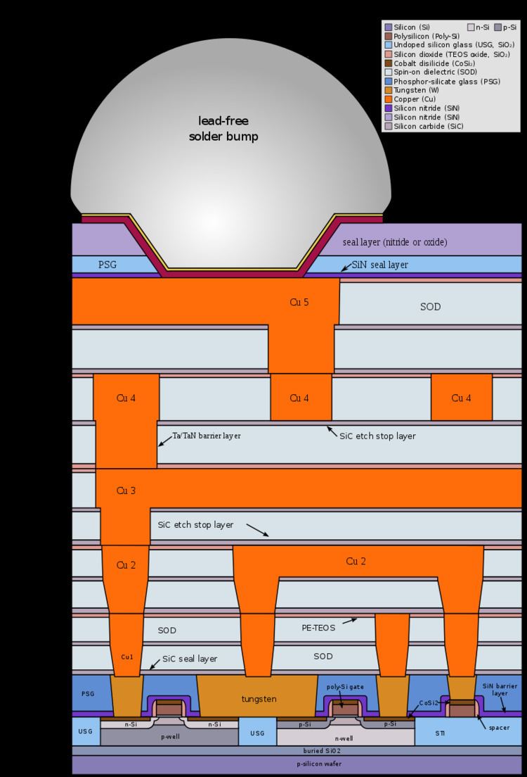
The back end of line (BEOL) is the second portion of IC fabrication where the individual devices (transistors, capacitors, resistors, etc.) get interconnected with wiring on the wafer, the metalization layer. Common metals are copper interconnect and aluminum interconnect. BEOL generally begins when the first layer of metal is deposited on the wafer. BEOL includes contacts, insulating layers (dielectrics), metal levels, and bonding sites for chip-to-package connections.
After the last FEOL step, there is a wafer with isolated transistors (without any wires). In BEOL part of fabrication stage contacts (pads), interconnect wires, vias and dielectric structures are formed. For modern IC process, more than 10 metal layers can be added in the BEOL.
The process used to form DRAM capacitors creates a rough and hilly surface, which makes it difficult to add metal interconnect layers and still maintain good yield. In 1998, state-of-the-art DRAM processes had 4 metal layers, while state-of-the-art logic processes had 7 metal layers.
As of 2002, 5 or 6 layers of metal interconnect are common.
As of 2009, typical DRAM devices (1 Gbit) use 3 layers of metal interconnect, tungsten on the first layer and aluminum on the higher layers.
As of 2011, many gate arrays are available with a 3-layer interconnect. Many power ICs and analog ICs use a 3-layer interconnect.
The top-most layers of a chip have the thickest and widest and most widely separated metal layers, which make the wires on those layers have the least resistance and smallest RC time delay, so they are used for power distribution and clock distribution. The bottom-most metal layers of the chip, closest to the transistors, have thin, narrow, tightly-packed wires, used only for local interconnect. Adding layers can potentially improve performance, but adding layers also reduces yield and increases manufacturing cost.
Chips with a single metal layer typically use the polysilicon layer to "jump across" when one signal needs to cross another signal—such as the RCA CDP1802 and the 4004, giving effectively 2 layers of interconnections.
Many microprocessors were designed with two metal interconnect layers, both of them aluminum, including the 1987 CVAX and the 1989 Rigel.
Many high-performance microprocessors were designed with 3 metal interconnect layers, all of them aluminum. Those included several processors using the CMOS-3 process, including the 1992 Alpha 21064; and processors using the CMOS-6 process, including the 1996 StrongARM.
The AMD Athlon Thunderbird has 6 interconnect layers, the AMD Athlon Palomino has 7 interconnect layers, the AMD Athlon Thoroughbred A has 8 interconnect layers, and the AMD Athlon Thoroughbred B has 9 interconnect layers. The Intel Xeon Dunnington has nine copper interconnect layers.
Steps of the BEOL:
- Silicidation of source and drain regions and the polysilicon region.
- Adding a dielectric (first, lower layer is Pre-Metal dielectric, PMD - to isolate metal from silicon and polysilicon), CMP processing it
- Make holes in PMD, make a contacts in them.
- Add metal layer 1
- Add a second dielectric (this time it is Intra-Metal dielectric)
- Make vias through dielectric to connect lower metal with higher metal. Vias filled by Metal CVD process.
- Add final passivation layer to protect the microchip
Before 1998, practically all chips used aluminum for the metal interconnection layers.
The four metals with the highest electrical conductivity are silver with the highest conductivity, then copper, then gold, then aluminum.
After BEOL there is a "back-end process" (also called post-fab), which is done not in the cleanroom, often by a different company. It includes wafer test, wafer backgrinding, die separation, die tests, IC packaging and final test.