
 | ||
An antiphase domain (APD) is a type of crystallographic defect in which the atoms in a region of a crystal are configured in the opposite order to those in the perfect lattice system. In other words, an APD is a region formed from antisite defects of a parent lattice. Crucially, crystals on either side of an antiphase domain boundary are related by a translation, rather than a reflection (a crystal twin) or an inversion (an inversion domain). In general, APDs form antiphase boundaries (APBs) with the parent lattice. Confusion between inversion domains and antiphase domains is common, even in the published literature, and particularly in the case of GaAs grown on silicon. (Similar defects form in GaN on silicon, where they are correctly identified as inversion domains). An example is illustrated in the diagram below.
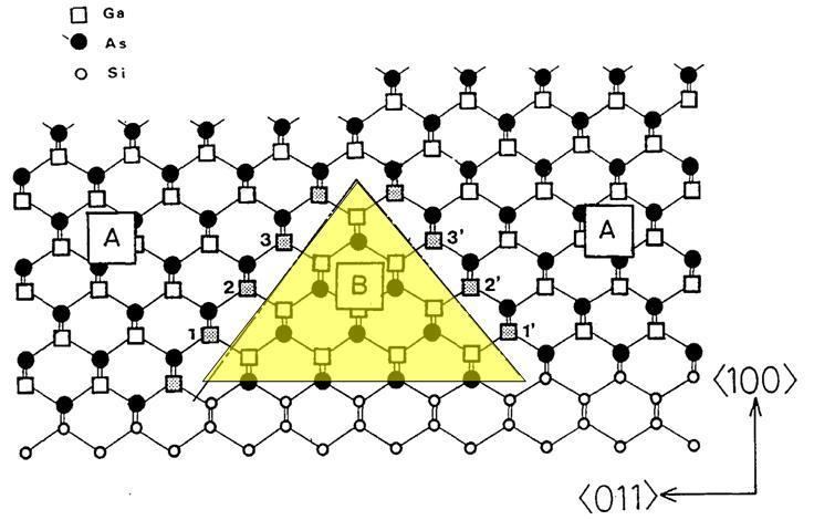
Figure 1. Highlighted area showing an inversion domain, incorrectly called an antiphase domain, in GaAs on Si.
(figures courtesy of JJJAP, VOL. 26, No.6, JUNE, 1987, pp. L944-L946)
The shaded region, B, is an example of an APD. In the figure, GaAs is grown on a misoriented surface of Si (details are not discussed here). The misorientation causes the Ga and As atoms in region B to be on opposite sites compared to the crystal matrix. The presence of the APD results in Ga sites 1, 1’, 2, 2’, 3, 3’ being bonded to Ga atoms in the APD to form an APB.
In mixed oxidation state materials like magnetite, antiphase domains and antiphase domain boundaries can occur as a result of charge-ordering even though there are no changes in atom locations. For example, the reconstructed magnetite (100) surface contains alternating FeII pairs and FeIII pairs in the first subsurface layer. An antiphase domain boundary can form if two subsurface FeII pairs meet when two terraces grow together.